
Controlling the content of specific desired memory elements when testing integrated circuits using sequential scanning techniques

a technology of sequential scanning and memory elements, applied in the field of integrated circuit testing, can solve problems such as inability to adapt to at least some environments, and inability to use the integrated circuit in a certain way

Active Publication Date: 2005-12-27
TEXAS INSTR INC
View PDF5 Cites 0 Cited by
  • Summary
  • Abstract
  • Description
  • Claims
  • Application Information

AI Technical Summary

Benefits of technology

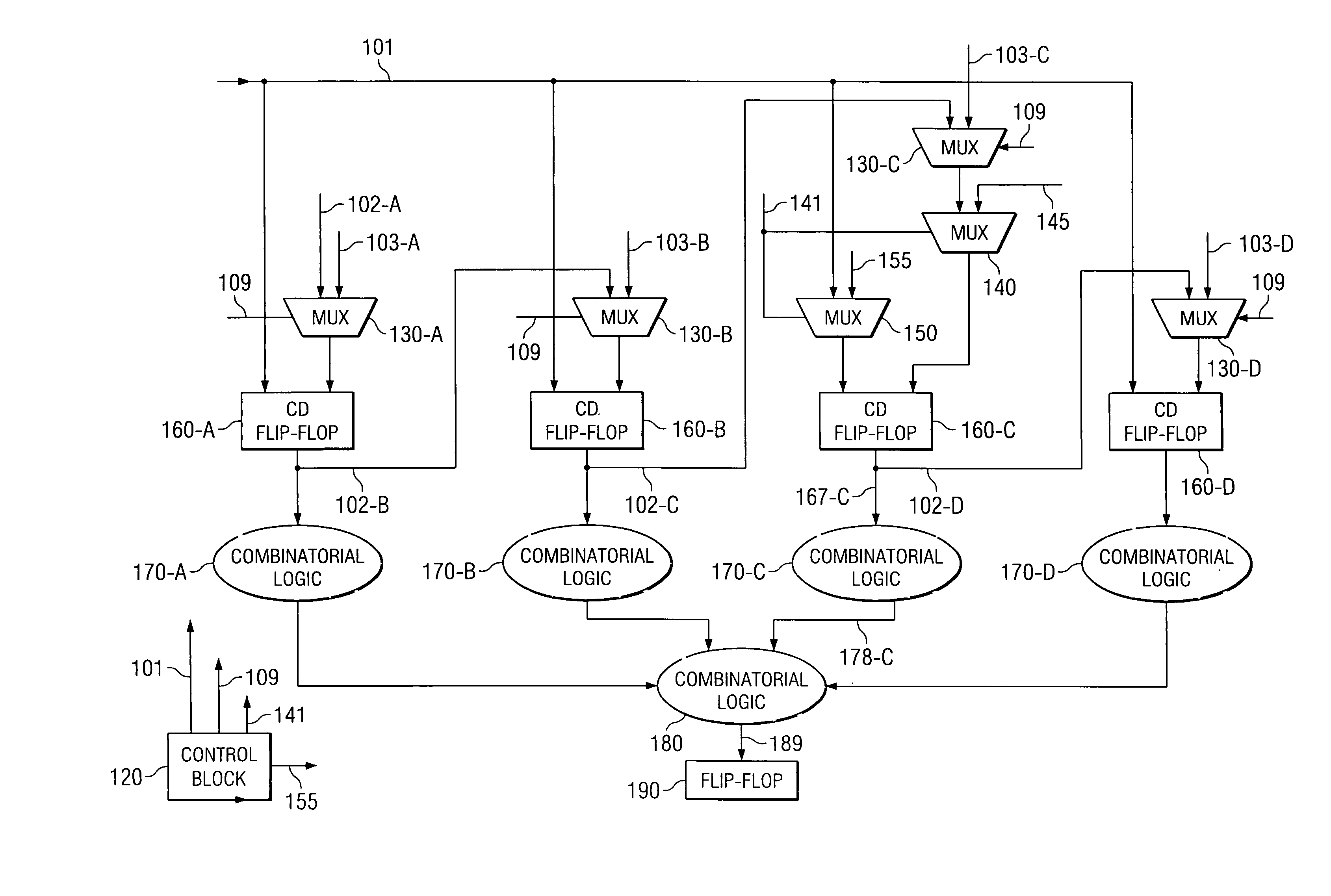
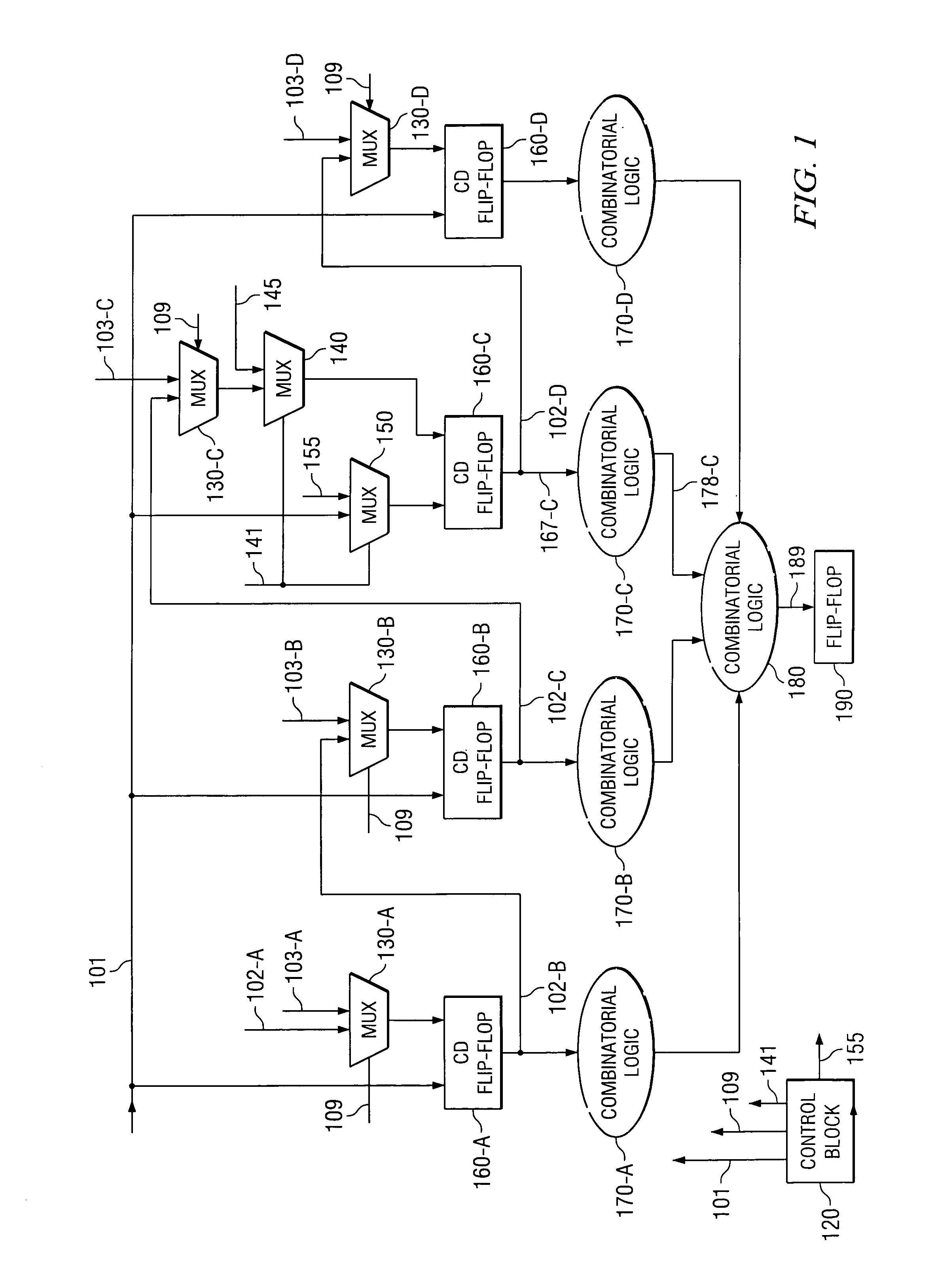
[0014]An aspect of the present invention allows the efficient testing of an integrated circuit containing memory elements. Each memory element contains a data input and an output. The memory elements may be connected sequentially in that the output of each memory element is coupled to a data input of a next memory element (except that the output of the last memory element would not be connected to other memory elements).
[0017]Due to the control provided by the launch multiplexor, a desired bit may be stored any time in the corresponding memory element. As a result, a designer is generally provided more flexibility in determining the specific sequence in which to connect the memory elements.

Problems solved by technology

One problem with such an approach is that the approach imposes (or requires) a specific order in which the memory elements are to be connected, and the corresponding connectivity requirement may pose challenges in layout and routing while designing an integrated circuit.
In addition, different tests may require conflicting paths Accordingly, the approach may not be suitable for at least some environments.
However, one disadvantage of such an approach is that a large number of memory elements may be required to support, for example, excitation of various paths, and the resulting consumption of space (on the integrated circuit) and power consumption may be unacceptable.

Method used


Image

  • Controlling the content of specific desired memory elements when testing integrated circuits using sequential scanning techniques
  • Controlling the content of specific desired memory elements when testing integrated circuits using sequential scanning techniques
  • Controlling the content of specific desired memory elements when testing integrated circuits using sequential scanning techniques

Examples


Embodiment Construction

1. Overview and Discussion of the Invention

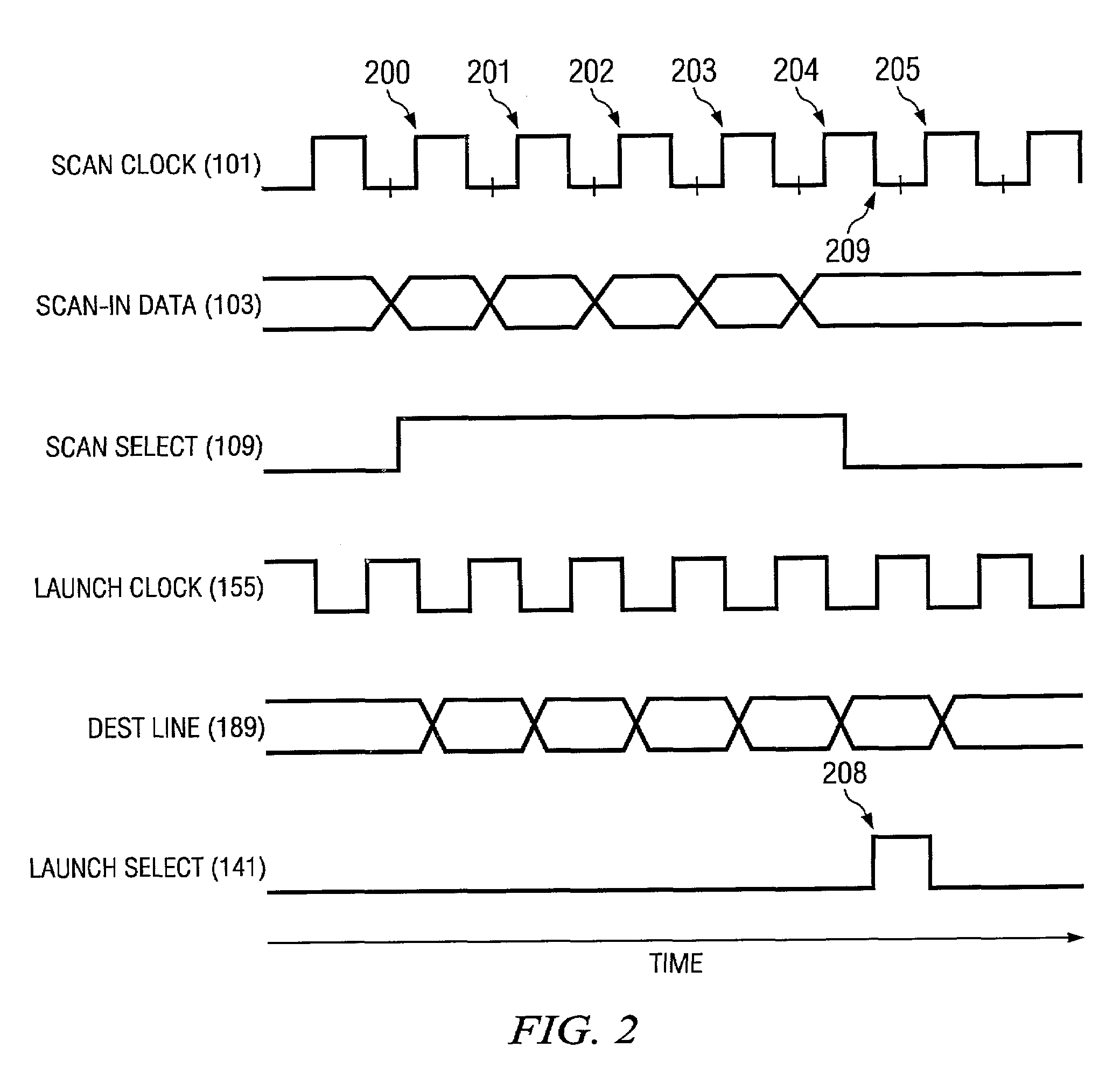
[0024]An aspect of the present invention enables a multiplexor to be associated with a specific memory element, the content of which is sought to be controlled. Thus, when testing an integrated circuit containing the specific memory element using sequential scanning technique, the multiplexor may be used to store the specific desired bit values in the specific memory element. The multiplexor may also enable bits of the test patterns to be stored in the specific memory element. Thus, the output(s) of an integrated circuit may be evaluated using a test pattern, the content of the specific memory element only can be changed, and the output(s) may be evaluated again after changing the content.

[0025]Several aspects of the invention are described below with reference to examples for illustration. It should be understood that numerous specific details, relationships, and methods are set forth to provide a full understanding of the invention. One s...


PUM


Abstract

A launch multiplexor which enables a desired bit to be stored into a desired memory element when using sequential scanning techniques (e.g., automatic test pattern generation (ATPG)). The launch multiplexor may be employed in addition to a scan multiplexor, which enables the test pattern bits or normal operating input to be selected and stored in the desired memory element. The scan multiplexor is used to scan-in a test pattern and evaluate a first input, and the launch multiplexor provides the control to store a desired bit into the corresponding memory element. Another output may be evaluated after storing the desired bit. In an embodiment, launch multiplexors are used associated with only memory elements in the critical paths, and the delay in transitioning from one output to another may be conveniently measured.

Description

BACKGROUND OF THE INVENTION[0001]1. Field of the Invention[0002]The present invention relates to testing of integrated circuits, and more specifically to a method and apparatus for controlling the content of specific desired memory elements when testing integrated circuits using a sequential scanning technique such as Automatic Test Pattern Generation (ATPG).[0003]2. Related Art[0004]Integrated circuits are often tested to verify whether the circuits operate in a desired manner. For example, an integrated circuit may be tested to ensure that each component (within the integrated circuit) generates a desired output in response to corresponding inputs, and such testing is often referred to as functional testing.[0005]Similarly, the delays in various paths of an integrated circuit may be measured to ensure that the paths generate the respective outputs within any time limits as may be necessary for the operation of the integrated circuit at a desired clock frequency, and such testing i...

Claims


Application Information

Patent Timeline
IPC IPC(8): G11C29/10G11C29/48
CPCG11C29/10G11C29/48G11C2029/3202
Inventor GUPTE, AJIT D.ABRAHAM, JAIS
Owner TEXAS INSTR INC
Learn More