Individually electrically addressable vertically aligned carbon nanofibers on insulating substrates

a technology of carbon nanofibers and individual electrical addresses, applied in the field of materials and nanotechnology, can solve the problems of not being able to achieve the goal of electrically conductive individual vacnfs on substrates, no process has been reported to achieve this goal, and the electrodes themselves are still rather large compared to the siz

a technology of carbon nanofibers and individual electrical addresses, applied in the field of materials and nanotechnology, can solve the problems of not being able to achieve the goal of electrically conductive individual vacnfs on substrates, no process has been reported to achieve this goal, and the electrodes themselves are still rather large compared to the siz

US6982519B2Inactive Publication Date: 2006-01-03THE UNITED STATES AS REPRESENTED BY THE DEPARTMENT OF ENERGY

Image

  • Individually electrically addressable vertically aligned carbon nanofibers on insulating substrates
  • Individually electrically addressable vertically aligned carbon nanofibers on insulating substrates
  • Individually electrically addressable vertically aligned carbon nanofibers on insulating substrates

Examples


example

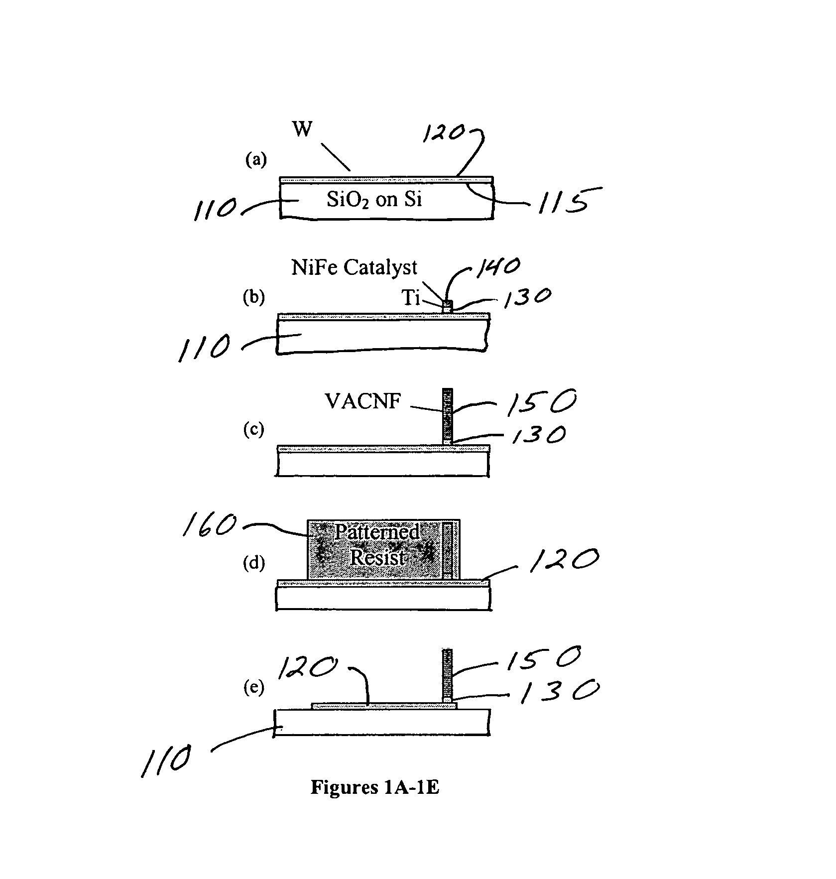
[0043]A specific embodiment of the invention will now be further described by the following, nonlimiting example which will serve to illustrate in some detail various features. The following example is included to facilitate an understanding of ways in which the invention may be practiced. It should be appreciated that the example which follows represents an embodiment discovered to function well in the practice of the invention, and thus can be considered to constitute the best mode for the practice of the invention. However, it should be appreciated that many changes can be made in the exemplary embodiment which is disclosed while still obtaining like or similar result without departing from the spirit and scope of the invention. Accordingly, the example should not be construed as limiting the scope of the invention.

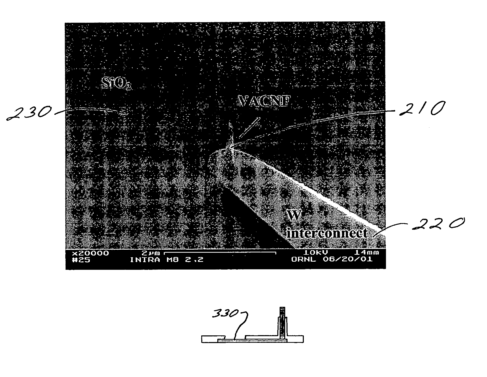
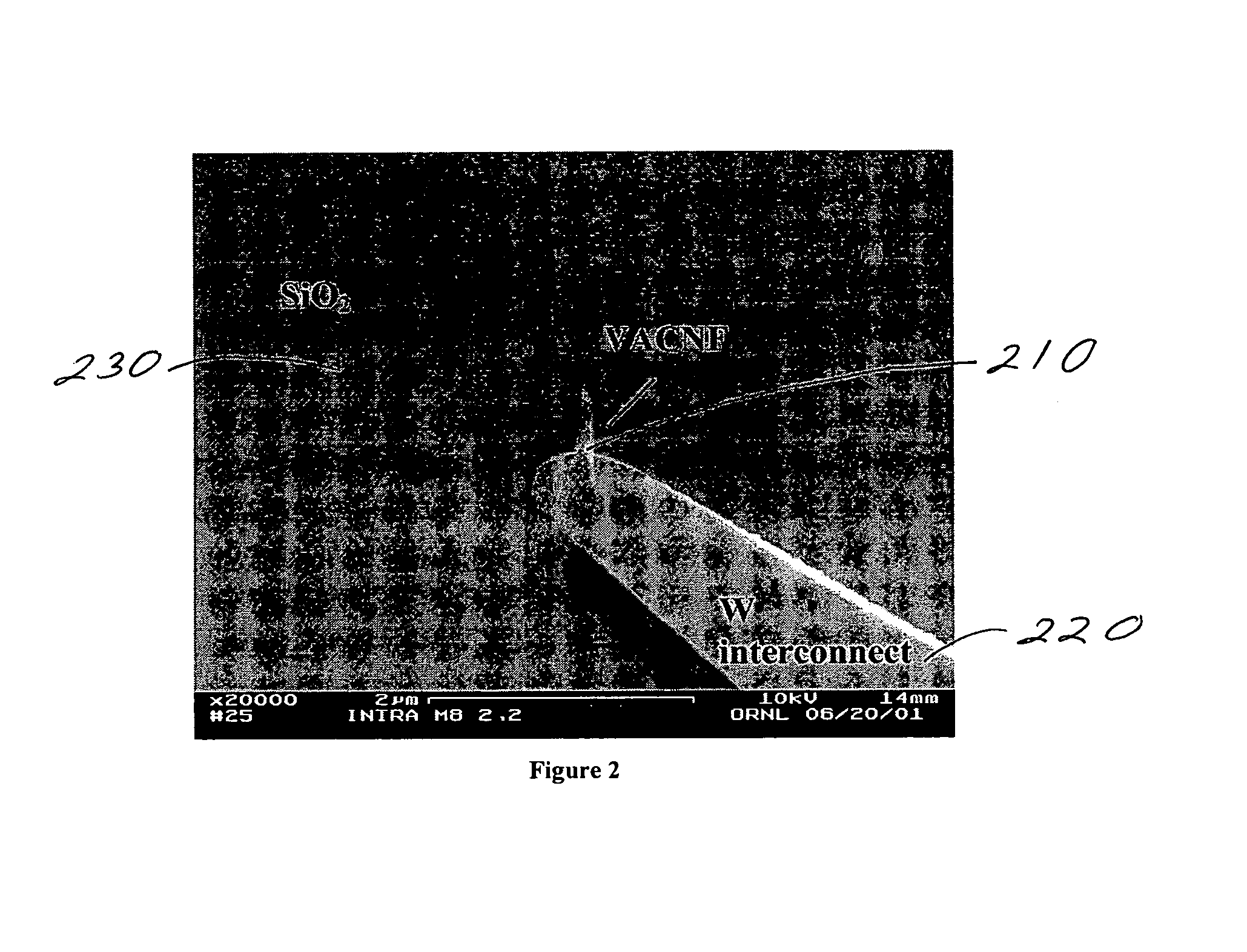
[0044]An exemplary fabrication process is summarized in FIGS. 1A–1E. In FIG. 1A, a silicon substrate 110 with an insulating silica surface 115 is coupled to a tungsten...


PUM

PropertyMeasurementUnit
radial distanceaaaaaaaaaa
lengthsaaaaaaaaaa
lengthsaaaaaaaaaa

Abstract

Systems and methods are described for individually electrically addressable carbon nanofibers on insulating substrates. An apparatus includes an electrically conductive interconnect formed on at least a part of an insulating surface on a substrate; and at least one vertically aligned carbon nanofiber coupled to the electrically conductive interconnect. A kit includes a substrate having an insulating surface; an electrically conductive interconnect formed on at least a part of the insulating surface; and at least one vertically aligned carbon nanofiber coupled to the electrically conductive interconnect.

Description

CROSS-REFERENCE TO RELATED APPLICATION[0001]This application is related to and claims a benefit of priority under 35 U.S.C. 119(e) and / or 35 U.S.C. 120 from, U.S. Ser. No. 60 / 322,929, filed Sep. 18, 2001, now pending, the entire contents of which are hereby expressly incorporated by reference for all purposes.STATEMENT AS TO RIGHTS TO INVENTIONS MADE UNDER FEDERALLY-SPONSORED RESEARCH AND DEVELOPMENT[0002]This invention was made with United States Government support under contract to UT-Battelle, LLC. The Government has certain rights in this invention.BACKGROUND OF THE INVENTION[0003]1. Field of the Invention[0004]The invention relates generally to the fields of materials and nanotechnology. More particularly, the invention relates to at least one fiber on an electrically conductive interconnect located on an insulating surface of a substrate. Specifically, a preferred implementation of the invention relates to a plurality of individually electrically addressable vertically aligned...

Claims


Application Information

Patent Timeline
03 Jan 2006
Publication
US6982519B2
IPC
H01J1/05; H01J1/14; H01J19/06; D01F9/127; G01N27/30; G01N27/403; H01J1/304; H01J9/02
CPC
B82Y30/00; D01F9/127; H01J1/3042; H01J9/025; G01N27/308; B82Y10/00; Y10S977/939; H01J2201/30469
Inventors
GUILLORN, MICHAEL A.; MCKNIGHT, TIMOTHY ERIC