Semiconductor device having densely stacked semiconductor chips

a semiconductor chip and semiconductor technology, applied in solid-state devices, basic electric elements, electrical apparatus construction details, etc., can solve the problem of not being electrically connected to the conductive layer on the substrate, and achieve the effect of high-density packaging

Inactive Publication Date: 2006-01-10
RENESAS ELECTRONICS CORP
View PDF29 Cites 94 Cited by
  • Summary
  • Abstract
  • Description
  • Claims
  • Application Information

AI Technical Summary

Benefits of technology

[0007]Therefore, the object of the present invention is to solve such problems of conventional methods, and to provide a semiconductor device which enables the high-density packaging of semiconductor chips even of the same size.

Problems solved by technology

However, when semiconductor chips of the same size are densely mounted by a conventional method, the electrodes of an underlying semiconductor chip are always hidden by the die-bonded overlying semiconductor chip, and cannot be electrically connected to conductive layers on the substrate.

Method used


Image

  • Semiconductor device having densely stacked semiconductor chips
  • Semiconductor device having densely stacked semiconductor chips
  • Semiconductor device having densely stacked semiconductor chips

Examples


first embodiment

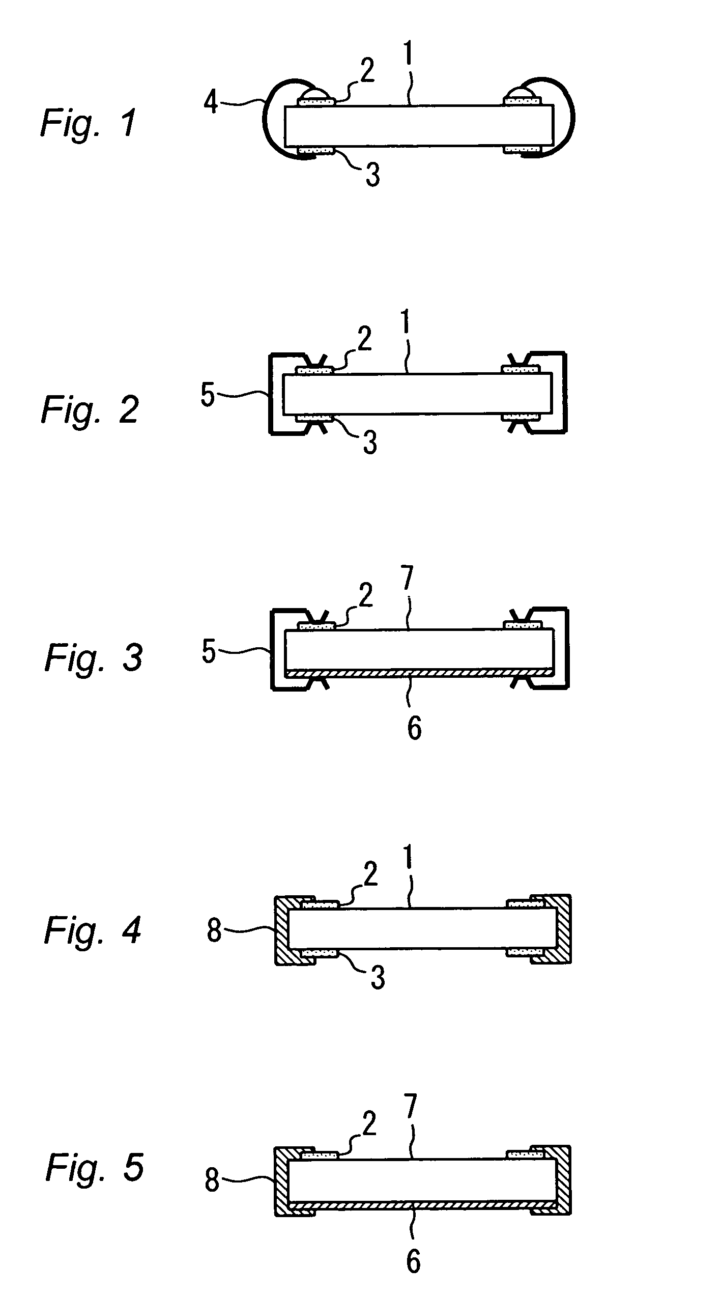
[0027]FIG. 1 is a sectional view showing a structure of a semiconductor device according to a First Embodiment.

[0028]In FIG. 1, reference numeral 1 indicates a semiconductor chip, 2 indicates a top-surface electrode (first electrode) formed on the top surface (first major surface) of the semiconductor chip 1, 3 indicates a back-surface electrode (second electrode) formed on the back surface (second major surface) of the semiconductor chip 1, and 4 indicates a conductive wire (conductor member) connecting the top-surface electrode 2 with the back-surface electrode 3.

[0029]The semiconductor device of this embodiment comprises a semiconductor chip 1 having electrodes 2 and 3 on the top and back surfaces, respectively, in which the top-surface electrode 2 is electrically connected with the back-surface electrode 3 by wire bonding.

[0030]This semiconductor device is produced by bonding an end of the conductive wire 4 to the top-surface electrode 2, inverting the semiconductor chip 1 upsid...

second embodiment

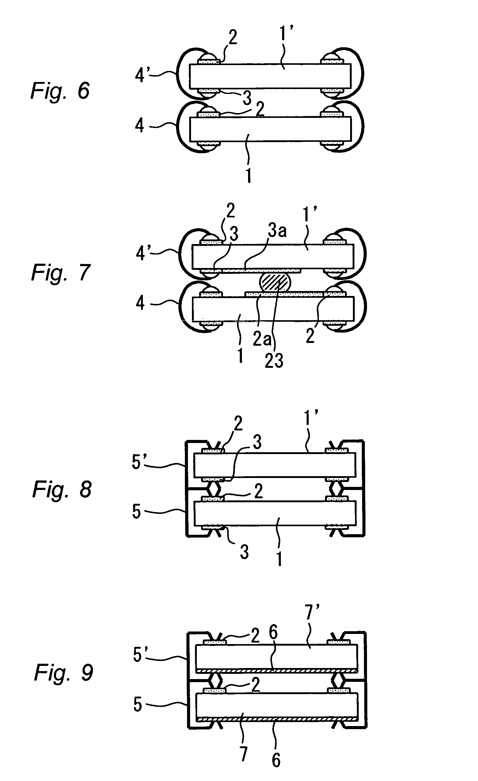
[0034]FIGS. 2 and 3 are sectional views showing structures of semiconductor devices according to a Second Embodiment.

[0035]In FIGS. 2 and 3, reference numeral 5 indicates a conductive clip having elasticity for clamping objects, 6 indicates an insulation layer provided by a surface insulation treatment, and 7 indicates a semiconductor chip having the insulation layer 6.

[0036]One of the semiconductor device of this embodiment comprises a semiconductor chip 1 having electrodes 2 and 3 on the top and back surfaces, respectively, and is provided with conductive clips 5 such that an end thereof contacts with the top-surface electrodes 2 and the other end contacts with the back-surface electrodes 3, and the connection of top- and back-surface electrodes 2 and 3 is retained by the elasticity thereof as FIG. 2 shows.

[0037]Alternatively, as FIG. 3 shows, another one of the semiconductor device of this embodiment comprises a semiconductor chip 7 having top-surface electrodes 2 and an insulati...

third embodiment

[0040]FIGS. 4 and 5 are sectional views showing structures of semiconductor devices according to a Third Embodiment.

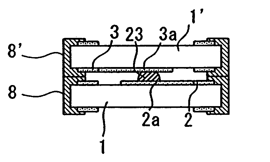
[0041]In FIGS. 4 and 5, reference numeral 8 indicates a conductive material injection-molded over the surfaces of the semiconductor chip 1, 7.

[0042]One of the semiconductor device according to this embodiment comprises a semiconductor chip 1 provided with electrodes 2 and 3 on the top and back surfaces, respectively, in which a conductive material 8 is injection-molded over the area from the top-surface electrodes 2 to the back-surface electrodes 3, as FIG. 4 shows.

[0043]Alternatively, as FIG. 5 shows, the other of the semiconductor device of this embodiment comprises a semiconductor chip 7 having electrodes 2 provided on the top surface and an insulation layer 6 provided on the back surface, in which a conductive material 8 is formed by injection molding or the like method over the area from the top-surface electrodes 2 to the insulation layer 6.

[0044]In other words, ...


PUM


Abstract

In a semiconductor chip having electrodes formed on the top surface, and electrodes or an insulation layer formed on the back surface, the top-surface electrodes are loop-connected with the back-surface electrodes by wire bonding, or, the top-surface electrodes are connected with the back-surface electrodes or an insulation layer by conductive clip, or by deposited conductive materials. The semiconductor chips thus produced are stacked, and wires, conductive clips, or conductive materials are connected and fixed to each other to produce a stacked semiconductor device in which semiconductor chips of the same size are densely packaged. Thus, a semiconductor device is provided which enables high-density packaging of semiconductor chips even of the same size.

Description

BACKGROUND OF THE INVENTION[0001]1. Field of the Invention[0002]The present invention relates to a semiconductor device having densely packaged semiconductor chips, in particular of the same size.[0003]2. Background Art[0004]FIG. 21 is a sectional view showing a structure of a conventional semiconductor device having stacked semiconductor chips.[0005]A conventional method for the high-density packaging of semiconductor chips will be described below. First, on a substrate 10q provided with conductive layers 10p, the largest chip 1p among semiconductor chips to be packaged is die-bonded with on-the-chip electrodes facing up. Similarly, a semiconductor chip 1q smaller than the semiconductor chip 1p previously bonded is die-bonded on the semiconductor chip 1p. However, the semiconductor chip to be die-bonded on the underlying semiconductor chip must always be die-bonded on the space where there are no electrodes of the underlying semiconductor chip. Next, the electrodes of each of thus ...

Claims


Application Information

Patent Timeline
Patent Type & Authority Patents(United States)
IPC IPC(8): H01L23/48H01L25/18H01L23/485H01L23/49H01L25/065H01L25/07
CPCH01L24/10H01L24/48H01L24/13H01L25/0657H01L2224/0401H01L2924/01033H01L2924/00014H01L2924/14H01L2924/014H01L2924/01004H01L2225/06572H01L2225/06527H01L2225/06524H01L2225/06506H01L2224/85399H01L2224/05599H01L2224/13099H01L2224/32145H01L2224/48091H01L2224/48145H01L2224/48465H01L2224/45099H01L2924/00H01L2224/13H01L2924/181H01L2924/00012
Inventor HARADA, KOZOSAWANO, HIROSHI
Owner RENESAS ELECTRONICS CORP
Why Eureka
Try Eureka