

Semiconductor package
a technology of semiconductors and packaging, applied in the direction of semiconductor devices, semiconductor/solid-state device details, electrical apparatus, etc., can solve the problems of low production yield, high production cost, and complicated transfer steps of insulating layers, etc., and achieve high production yield, high density packaging, and easy to use
- Summary
- Abstract
- Description
- Claims
- Application Information
AI Technical Summary
Benefits of technology
Problems solved by technology
Method used
Image

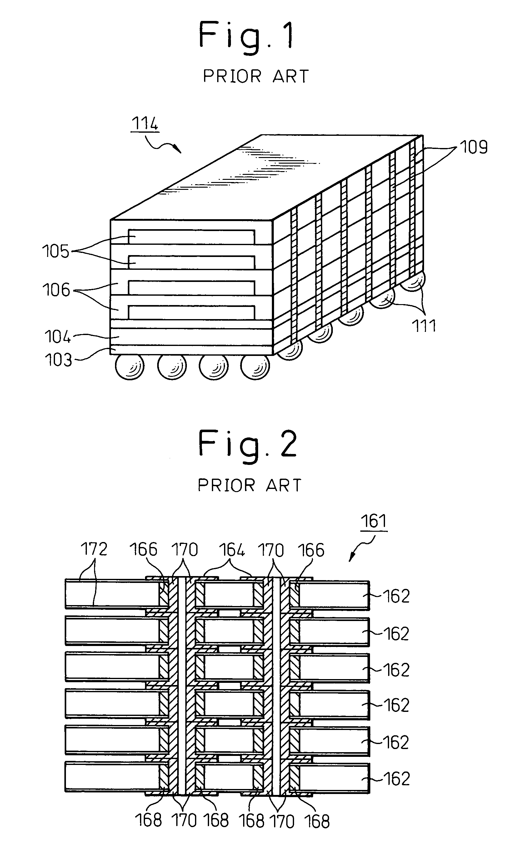
Examples
examples
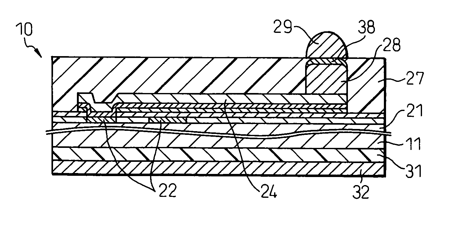
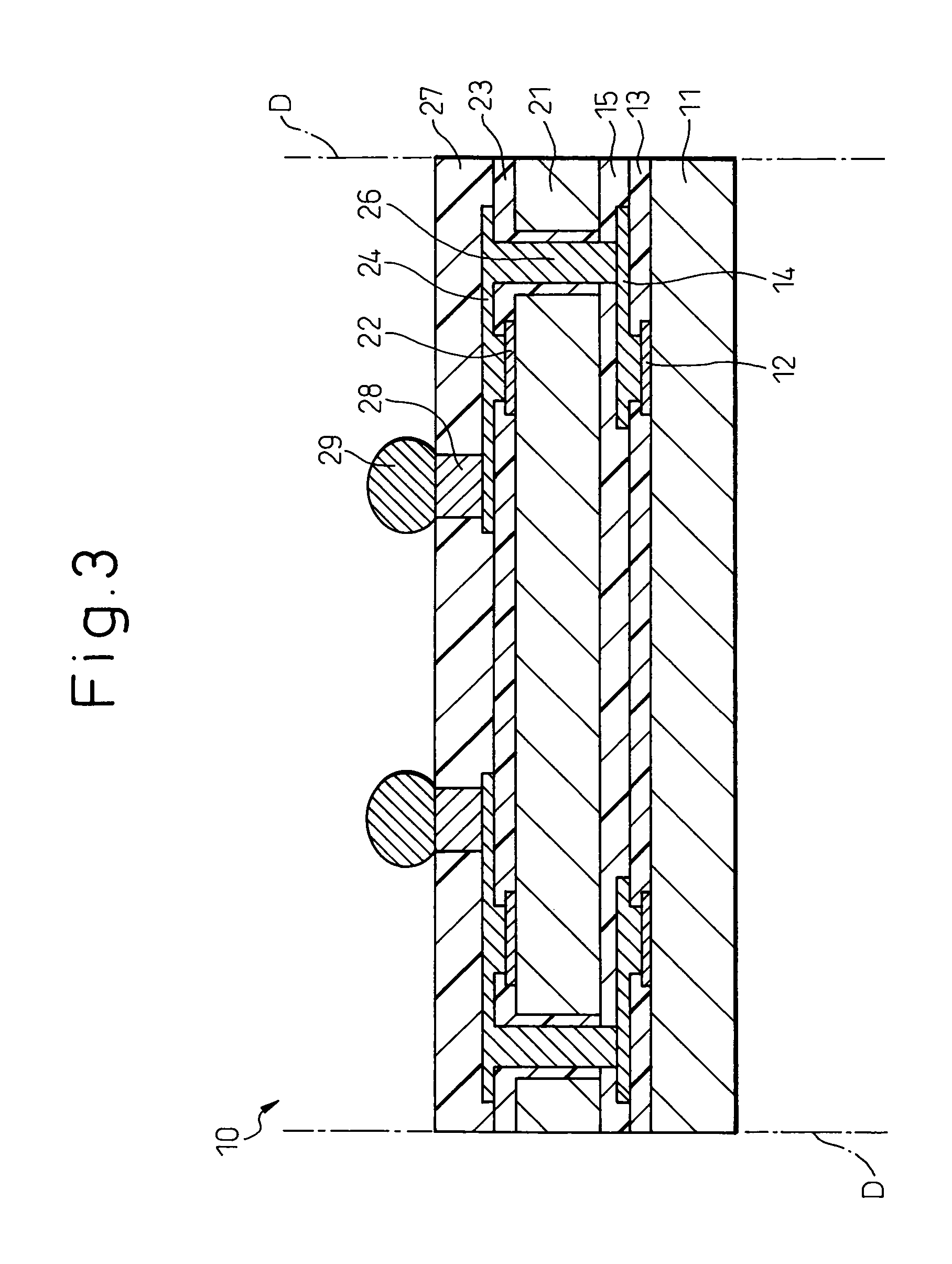
[0044]Next, examples of the invention will be explained with reference to the accompanying drawings. Note, however, that the invention is not limited to the following examples. In the following explanation of the production method of the semiconductor package, one semiconductor package is shown in magnification for the purpose of simplification of the explanation. In practice, however, as the production is performed in the wafer level, the production method that collectively and batchwise fabricates a large number of semiconductor packages into one wafer and dices the wafer into discrete semiconductor packages, is used.
[0045]FIG. 3 is a sectional view showing a preferred example of the semiconductor package according to the invention. The semiconductor package 10 is produced by fabricating a large number of semiconductor devices into a silicon wafer in accordance with a predetermined design and dicing the wafer along a dicing line “D”. In the illustrated semiconductor package 10, a ...
PUM
 Abstract
Description
Claims
Application Information