Manufacturing method package substrate

a manufacturing method and substrate technology, applied in the direction of printed element electric connection formation, conductive pattern formation, non-metallic protective coating application, etc., can solve the problems of difficult to realize fine pitches, circuit density drop, and missing bumps, so as to reduce the defect rate of bumps and uniform width and height

Inactive Publication Date: 2007-12-27
SAMSUNG ELECTRO MECHANICS CO LTD
View PDF2 Cites 13 Cited by
  • Summary
  • Abstract
  • Description
  • Claims
  • Application Information

AI Technical Summary

Benefits of technology

[0011]An aspect of the invention is to provide a manufacturing method of a package substrate which enables fine pitch of bumps for electrical connection with an electronic chip on a package substrate and allows uniform widths and heights, to lessen the defect rate of the bumps, and to realize high-density packages.

Problems solved by technology

Also, inferiorities such as missing bumps may occur, depending on the quality of the surface treatment, and it is difficult to realize fine pitches, due to the inability to obtain bump pitches below a certain dimension.
However, in order to apply electroplating to a package substrate, plating bus lines need to be included in the substrate design, whereby the circuit density is lowered, and the manufacturing of high-density circuit products becomes difficult.
After the electroplating has been completed, plating bus lines are cut by a router or by dicing, and in this process some plating bus lines may not be completely severed, to cause noises in the transmission of electrical signals due to the plating bus lines remaining on the package substrate.
This consequently deteriorates the electrical performance of the product.

Method used


Image

  • Manufacturing method package substrate
  • Manufacturing method package substrate
  • Manufacturing method package substrate

Examples


Embodiment Construction

[0025]The manufacturing method of package substrate according to certain embodiments of the invention will be described below in more detail with reference to the accompanying drawings, in which those components are rendered the same reference number that are the same or are in correspondence, regardless of the figure number, and redundant explanations are omitted.

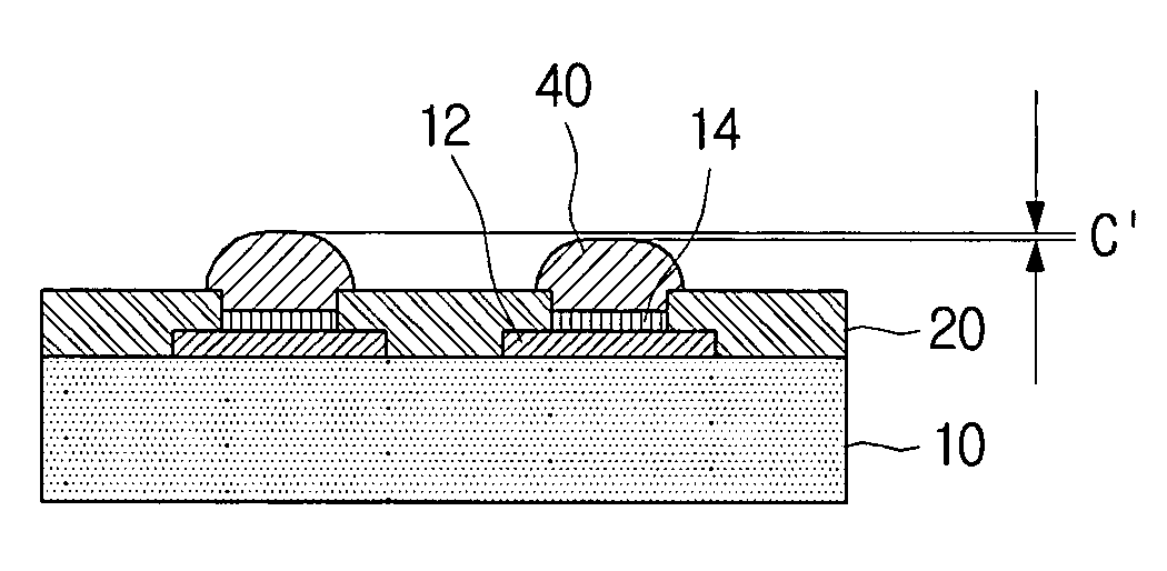
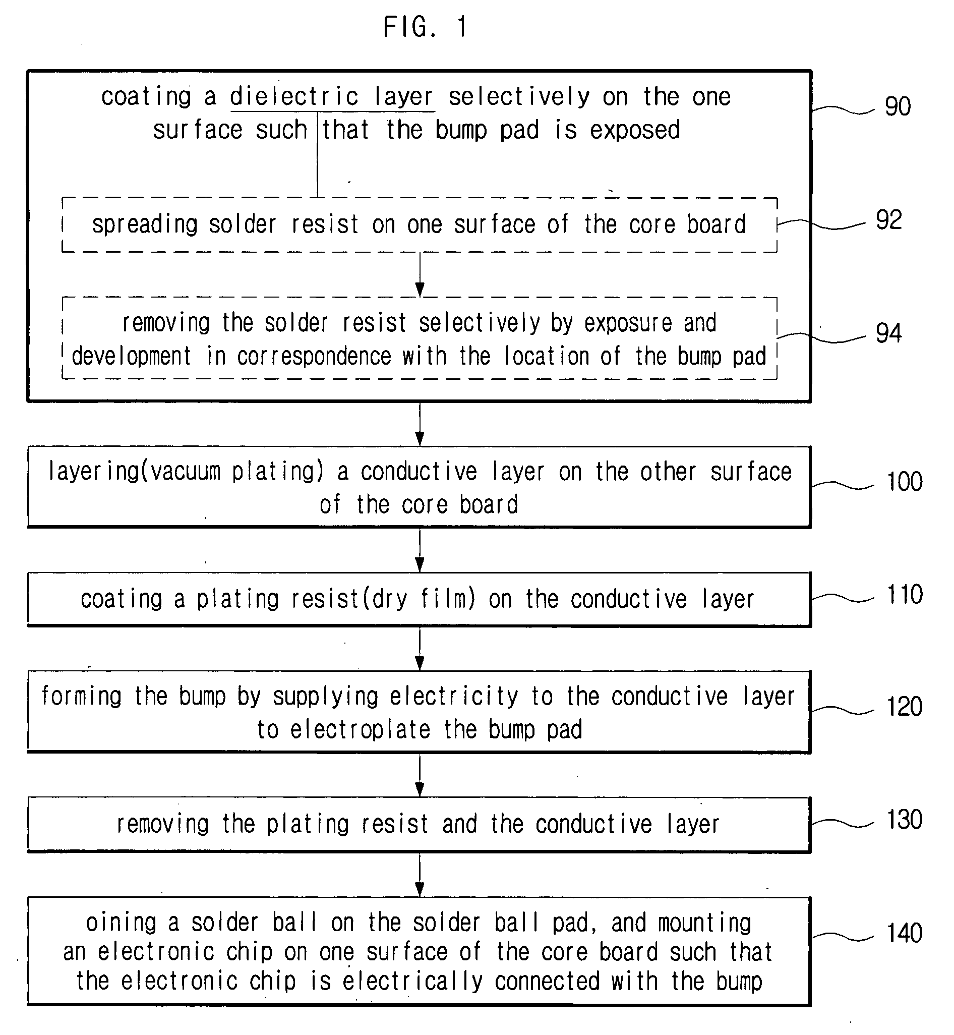
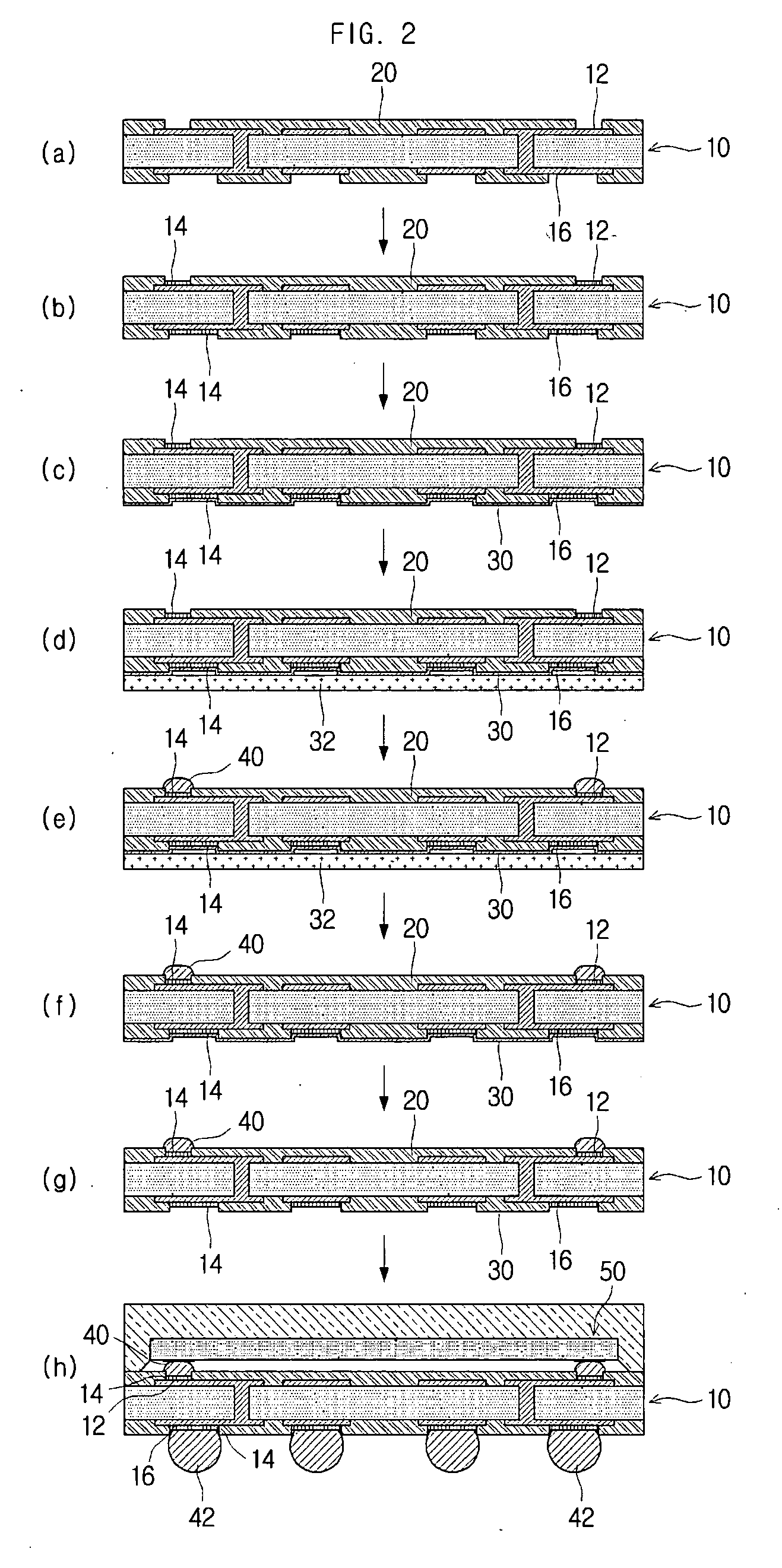
[0026]FIG. 1 is a flow chart illustrating a manufacturing method of a package substrate according to an embodiment of the present invention, FIG. 2 is a schematic diagram illustrating a manufacturing process of a package substrate according to an embodiment of the present invention, and FIG. 3 is a sectional view illustrating a package substrate according to an embodiment of the present invention. Referring to FIG. 2 and FIG. 3, a core board 10, bump pads 12, electroless plated layers 14, solder ball pads 16, solder masks 20, a conductive layer 30, a plating resist 32, bumps 40, solder balls 42, and an electronic chip 50 a...


PUM


Abstract

A manufacturing method of a package substrate is disclosed. The method for manufacturing a package substrate is by forming a bump on a bump pad in a core board, where a first circuit pattern including the bump pad is formed on one surface, a second circuit pattern electrically connected with the first circuit pattern is formed on the other surface, and a dielectric layer is selectively coated on the one surface such that the bump pad is exposed. The method includes layering a conductive layer on the other surface of the core board, coating a plating resist on the conductive layer, forming the bump by supplying electricity to the conductive layer to electroplate the bump pad, and removing the plating resist and the conductive layer. This makes it possible to omit the coining process and increase the density of the circuit by forming a fine bump by an electro tin plating method with small plating thickness deviation without designing additional plating bus lines, and improves the electrical performance without remaining plating bus lines.

Description

CROSS-REFERENCE TO RELATED APPLICATIONS[0001]This application claims the benefit of Korean Patent Application No. 10-2006-0055833 filed with the Korean Intellectual Property Office on Jun. 21, 2006, the disclosure of which is incorporated herein by reference in its entirety.BACKGROUND[0002]1. Technical Field[0003]The present invention relates to a manufacturing method of a package substrate.[0004]2. Description of the Related Art[0005]A package substrate is a printed circuit board such as an FCP-(Flip chip package), CSP (Chip scale package), and BGA (Ball grid array) used in an electronic package where electronic chips are mounted, and the pitch, precision, reliability, and cost, etc., of electric contact points between a package substrate and an electronic chip mounted on its surface are very important factors which determine the performance of the package.[0006]In the manufacturing process of a package substrate according to prior art, solder resist is first spread on the surface ...

Claims


Application Information

Patent Timeline
Patent Type & Authority Applications(United States)
IPC IPC(8): H01L21/00H01L21/44
CPCH01L21/4853H01L21/563H01L2924/00014H01L23/3128H01L23/49816H01L23/49838H01L2224/16225H01L2924/01078H01L2924/01079H01L2924/15311H05K3/243H05K3/28H05K3/3473H05K3/42H05K2203/043H05K2203/054H05K2203/1581H01L2224/05573H01L2224/05568H01L2224/05599H05K3/12
Inventor LEE, JONG-JINKIM, SUN-MOONSHIN, MI-SEONLEE, YONG-BIN
Owner SAMSUNG ELECTRO MECHANICS CO LTD
Why Eureka
Try Eureka