Stacked semiconductor device

a semiconductor chip and stacking technology, applied in semiconductor devices, semiconductor/solid-state device details, instruments, etc., can solve the problems of limited number of bonding wires that can be used on the chip, inaccessible pads for bonding wires, and certain limitations of efforts to reduce the size of transistors used in semiconductor devices, etc., to achieve a high yield

Active Publication Date: 2008-04-01
NEC CORP +1
View PDF14 Cites 37 Cited by
  • Summary
  • Abstract
  • Description
  • Claims
  • Application Information

AI Technical Summary

Benefits of technology

[0014]It is therefore an object of the present invention to provide a stacked semiconductor device which can be manufactured at a high yield regardless of through-connection failures.
[0019]According to the present invention, provision of a plurality of through-connections, which include, for example, backup through-connections that provide a redundant structure for primary through-connections, are effective to reduce the fraction defective of the stacked semiconductor device that is made up of a plurality of semiconductor chips, due to a failure of the through-connections. Therefore, the yield of stacked semiconductor devices is prevented from being lowered, but can be increased.

Problems solved by technology

It is understood that there are certain limitations on the efforts to reduce the size of transistors used in semiconductor devices.
(1) Because a pad provided on the surface of a chip needs a certain pad area such as 100 μm squared, the number of bonding wires that can be used on the chip is limited;
(2) Since pads disposed on the surfaces of stacked semiconductor chips are required to be positioned on outer edges of the stacked semiconductor chips so that they can be connected from outside of the chips, pads for bonding wires are not accessible if the stacked semiconductor chips are identical in shape to each other.
Because of these steps, it is generally difficult to increase the accuracy with which to form through-connections, and hence the yield of through-connections has been low.
If three or more semiconductor chips are stacked, then since through-connections need to be positioned accurately between the stacked semiconductor chips, the yield of products made up of stacked semiconductor chips is also low.
In addition, when the number of stacked semiconductor chips is increased, e.g., three or four semiconductor chips are stacked, if even one of the stacked semiconductor chips suffers a through-connection failure, then the entire stacked semiconductor device becomes defective.
Since the effect that a through-connection failure on one semiconductor chip has on a defect of a stacked semiconductor device increases depending on the number of stacked semiconductor chips, the fraction defective of stacked semiconductor devices increases as the number of stacked semiconductor chips increases.

Method used


Image

  • Stacked semiconductor device
  • Stacked semiconductor device
  • Stacked semiconductor device

Examples


Embodiment Construction

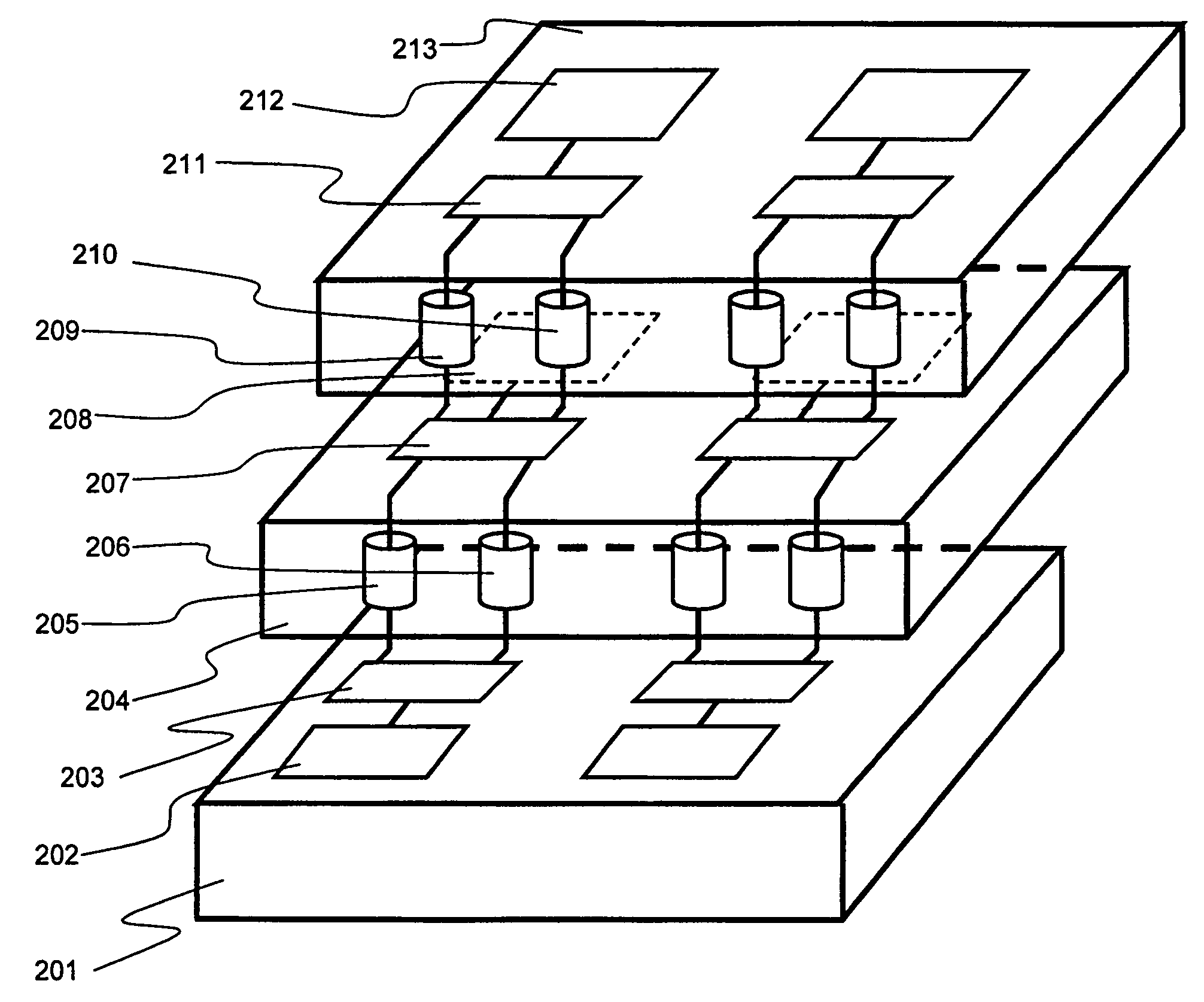
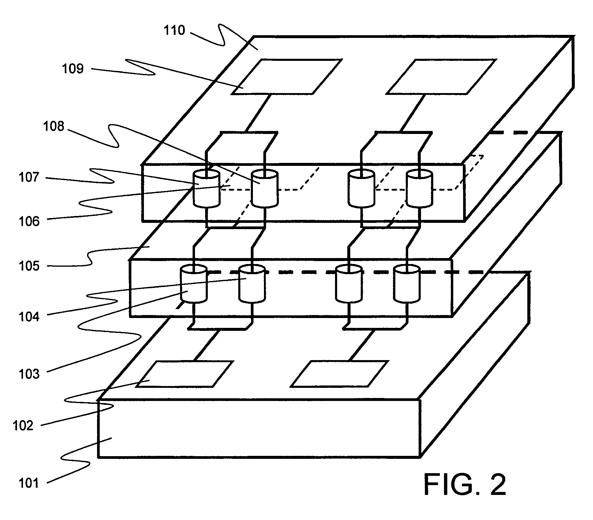
[0039]A stacked semiconductor device according to an embodiment of the present invention as shown in FIG. 2 has three semiconductor chips 101, 105, 110. Second semiconductor chip 105 and third semiconductor chip 110 are stacked, successively in the order named, on first semiconductor chip 101.

[0040]First functional circuit 102 is disposed on first semiconductor chip 101, second functional circuit 106 on second semiconductor chip 105, and third functional circuit 109 on third semiconductor chip 110. These functional circuits 102, 106, 109 are electrically connected by through-connection 103 extending through second semiconductor chip 105 and through-connection 107 extending through third semiconductor chip 110. Backup through-connection 104 extends through second semiconductor chip 105 parallel to through-connection 103, and backup through-connection 108 extends through third semiconductor chip 110 parallel to through-connection 107. Backup through-connections 104, 108 are connected ...


PUM


Abstract

A stacked semiconductor device includes a plurality of semiconductor chips and a conductive path extending through at least one of the semiconductor chips. The semiconductor chips are stacked together. The semiconductor chips are electrically connected by the conductive path, and the conductive path has a plurality of through-connections extending through the corresponding semiconductor chip.

Description

BACKGROUND OF THE INVENTION[0001]1. Field of the Invention[0002]The present invention relates to a semiconductor device such as a semiconductor integrated circuit device or the like, and more particularly to a semiconductor device comprising a plurality of stacked semiconductor chips.[0003]2. Description of the Related Art[0004]Semiconductor integrated circuit devices have an integration density increased as the size of transistors that make up semiconductor integrated circuit devices decreases. Circuits for achieving many functions are installed on semiconductor integrated circuit devices each comprising a single semiconductor chip. Semiconductor memory devices, regardless of the types of memory circuits such as DRAMs (Dynamic Random Access Memories), SRAMs (Static Random Access Memories), or the like, also have a storage capacity increased as the size of transistors that make up semiconductor memory devices decreases.[0005]In recent years, however, there have been growing demands ...

Claims


Application Information

Patent Timeline
Patent Type & Authority Patents(United States)
IPC IPC(8): H01L29/40
CPCG11C5/02G11C5/04H01L23/525H01L25/0657H01L23/481H01L2224/16145H01L2225/06513H01L2924/13091H01L2225/06527H01L2225/06541H01L2924/3011H01L2924/01019H01L2924/00
Inventor FUKAISHI, MUNEOSAITO, HIDEAKIHAGIHARA, YASUHIKOMIZUNO, MASAYUKIIKEDA, HIROAKISHIBATA, KAYOKO
Owner NEC CORP
Why Eureka
Try Eureka