
Addressing of AC plasma display

a plasma display and ac technology, applied in the field of addressing of ac plasma displays, can solve the problems of shortening the life adding to the cost of electronic circuitry, and the multi-color columnar discharge pdp with phosphors has not been successfully commercialized in the pdp industry, so as to reduce the background glow, improve the wall charge profile, and reduce the effect of phosphor and pdp degradation

Inactive Publication Date: 2006-01-10
IMAGING SYST TECH
View PDF34 Cites 13 Cited by
  • Summary
  • Abstract
  • Description
  • Claims
  • Application Information

AI Technical Summary

Benefits of technology

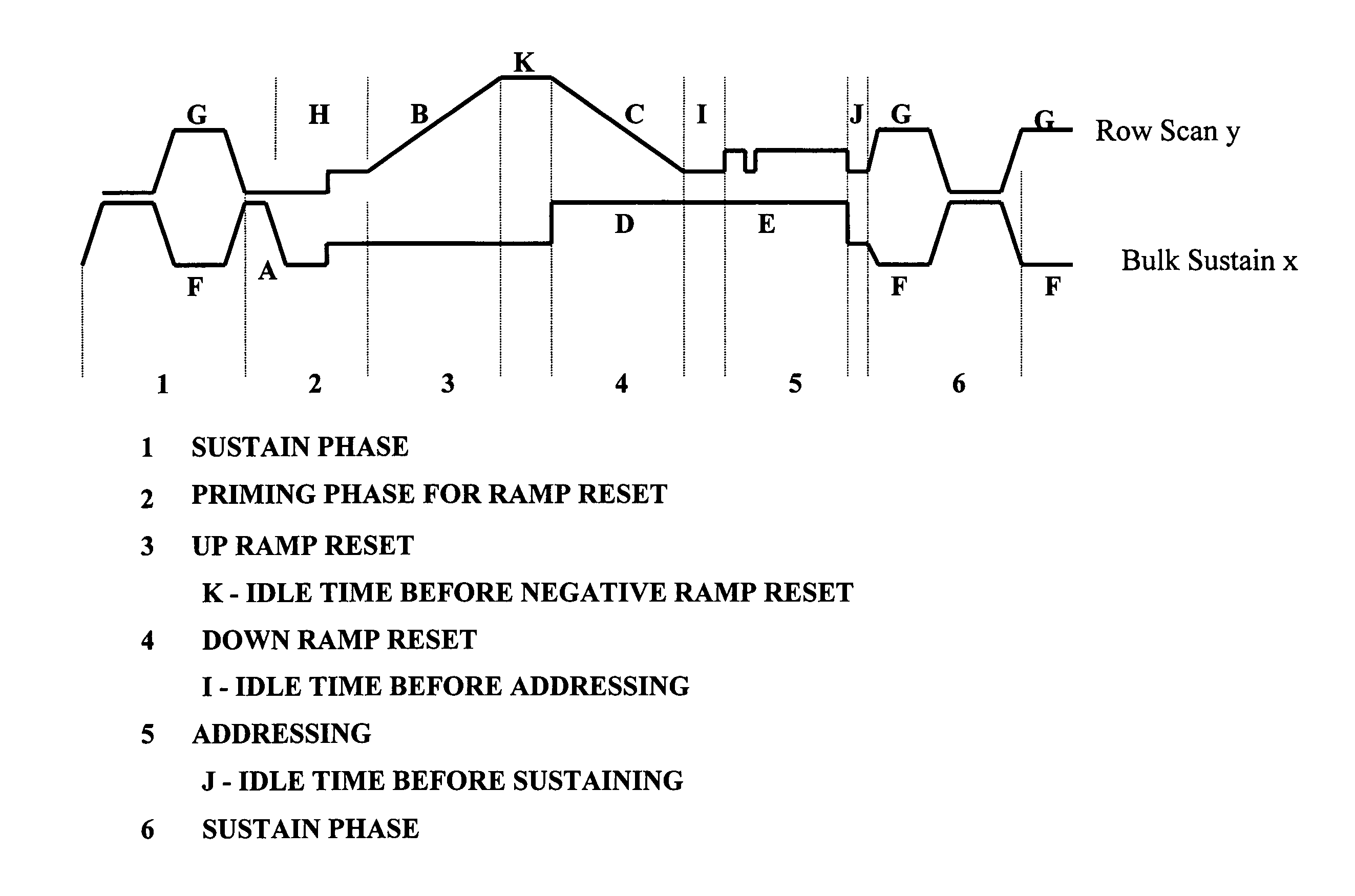
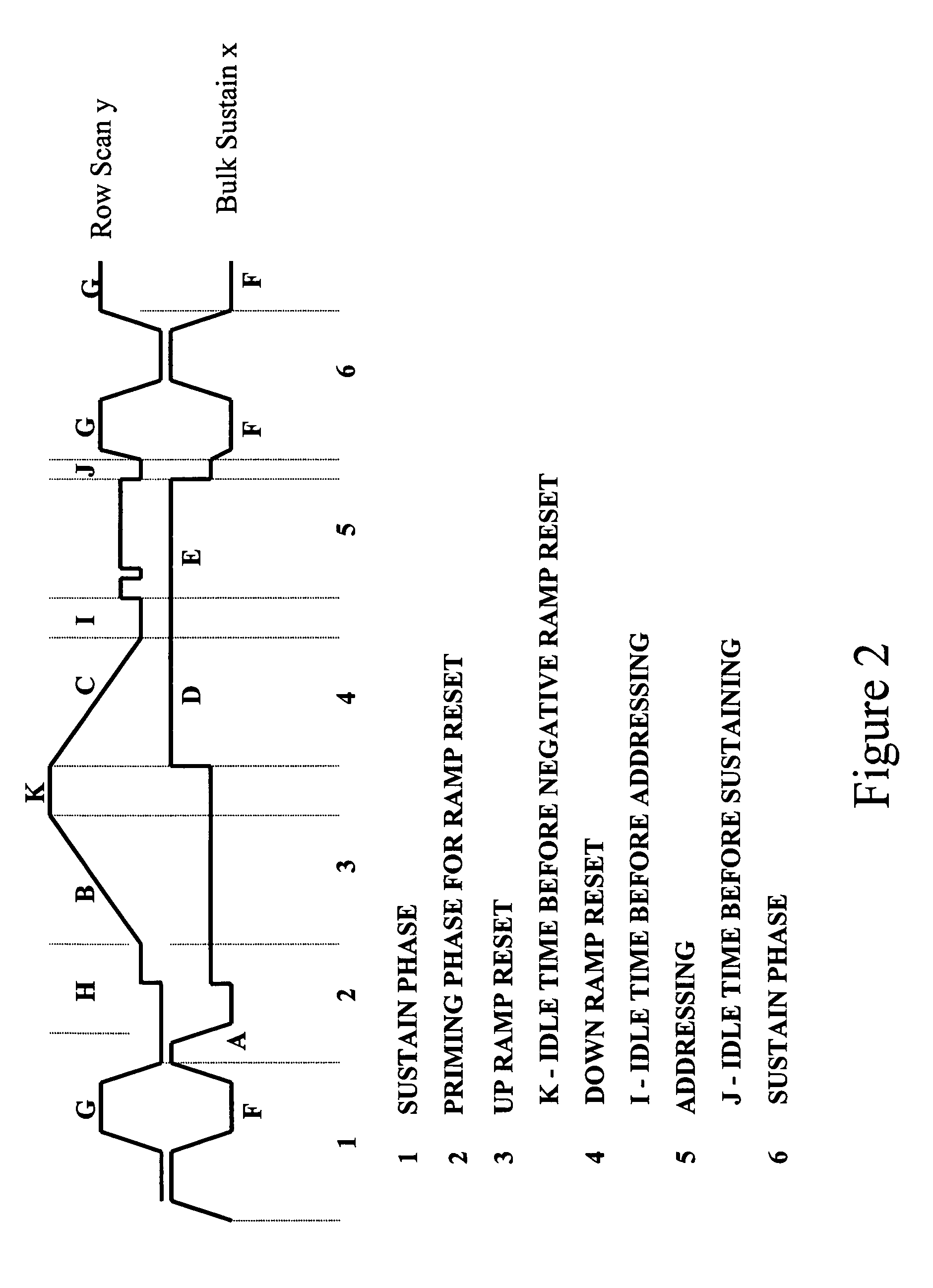
[0047]SAS allows for simultaneous addressing and sustaining thereby providing more time within the frame for other waveform operations. By comparison the ADS architecture of Fujitsu allocates 75 percent of the frame time for addressing and 25 percent for sustaining.
[0048]Because both the addressing and sustaining are completed in 75 percent of the available frame time, SAS has 25% remaining frame time.
[0049]SAS has the ability to do 12 to 17 sub-fields for panel resolutions up to 768 row scan electrodes and 10 to 12 sub-fields for resolutions of 1080 row scan electrodes without using dual scan.
[0050]As noted above slow reset ramp can also be used with SAS. The slow ramp reset can be tailored to ramp slopes of 1.5 microseconds per volt or less which greatly minimizes background glow. This is not possible with the ADS approach of Fujitsu. SAS also provides for a more uniform contrast rati

Problems solved by technology

The discharge between the two opposite electrodes generates electrons and ions that bombard and deteriorate the phosphor thereby shortening the life of the phosphor and the PDP.
For reasons discussed above and also as presented in TABLE I hereafter, the multi-color columnar discharge PDP with phosphors has not been successfully commercialized in the PDP industry.
The high peak discharge current of columnar discharge greatly adds to the costs of the electronic circuitry.
However, a protective overcoat decreases light output from the phosphor.
Because the entire reset cycle time of Habino et al. is a maximum of 360 microseconds, it is not feasible for Habino et al to use a reset ramp slope of 1.5 volts per microsecond without also decreasing the maximum or peak voltage amplitude of the reset voltage below the amplitude required for reliable discharge and stable addressing.
This is not possible with the ADS approach of Fujitsu.
It is more costly to use dual scan because of the added electronics and reduced PDP yield.

Method used


Image

  • Addressing of AC plasma display
  • Addressing of AC plasma display
  • Addressing of AC plasma display

Examples


Embodiment Construction

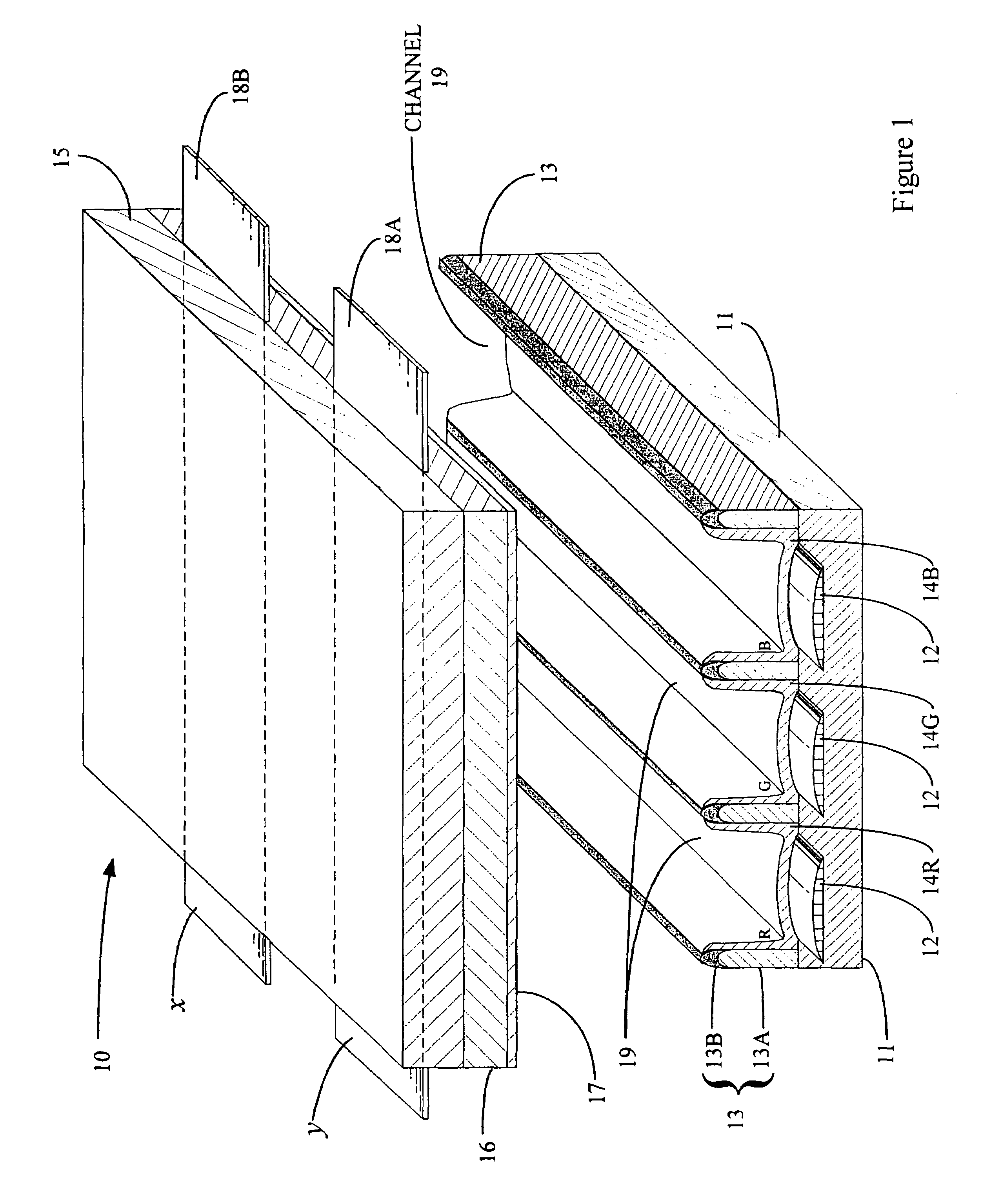
[0060]FIG. 1 shows an AC gas discharge plasma display panel with a surface discharge structure 10 similar to the surface discharge structure illustrated and described in FIG. 2 of U.S. Pat. No. 5,661,500 (Shinoda et al.) which is cited above and incorporated herein by reference. The panel structure 10 has a bottom or rear glass substrate 11 with column data electrodes 12, barriers 13, and phosphor 14R, 14G, 14B.

[0061]Each barrier 13 comprises a bottom portion 13A and a top portion 13B. The top portion 13B is dark or black for increased contrast ratio. The bottom portion 13A may be translucent, opaque, dark, or black.

[0062]The top substrate 15 is transparent glass for viewing and contains y row scan (or sustain) electrodes 18A and x bulk sustain electrodes 18B, dielectric layer 16 covering the electrodes 18A and 18B, and a magnesium oxide layer 17 on the surface of dielectric 16. The magnesium oxide is for secondary electron emission and helps lower the overall operating voltage of t...


PUM


Abstract

Addressing and sustaining of a surface discharge AC plasma display panel by applying addressing voltages to at least one section of the panel while at least one other section of the panel is being simultaneously sustained.

Description

RELATED APPLICATIONS[0001]This is a continuation in part under 35 USC 120 of a U.S. patent application Ser. No. 09 / 774,055 filed Jan. 31, 2001 now abandoned which is a continuation in part under 35 USC 120 of a U.S. patent application Ser. No. 09 / 643,843 filed Aug. 23, 2000 now abandoned which is a continuation in part under 35 USC 120 of U.S. patent application Ser. No. 09 / 556,337 filed Apr. 24, 2000 now abandoned which claims priority under 35 USC 119 (e) of Provisional Application 60 / 131,177 filed Apr. 26, 1999.INTRODUCTION[0002]This invention relates to the addressing and sustaining of an AC gas discharge plasma display panel (PDP) that uses a surface discharge structure. This invention comprises a method of operating an AC plasma display by applying selective write and / or selective erase voltages to at least one display section of a surface discharge PDP while at least one other display section of the PDP is being simultaneously sustained. This invention of Simultaneous Address...

Claims


Application Information

Patent Timeline
IPC IPC(8): G09G3/28G09G3/10
CPCG09G3/2927G09G3/2932G09G3/294G09G2310/066G09G2310/0216G09G2310/0221
Inventor VELAYUDHAN, BALA KWEDDING, CAROL A.GUY, JEFFREY W.
Owner IMAGING SYST TECH
Learn More