
Asynchronous request/synchronous data dynamic random access memory

Inactive Publication Date: 2001-03-27
RAMBUS INC
View PDF58 Cites 88 Cited by
  • Summary
  • Abstract
  • Description
  • Claims
  • Application Information

AI Technical Summary

Benefits of technology

One object of the invention is to provide a memory system with an improved balance between request-to-data latency, power consumption and bandwidth.
According to one aspect of the invention, a memory interface is provided that maintains the high-bandwidth of synchronous systems, while reducing the latency and power requirements of these systems. This is accomplished by using an asynchronous interface for the address and control information, and using a synchronous interface for fast data transport.
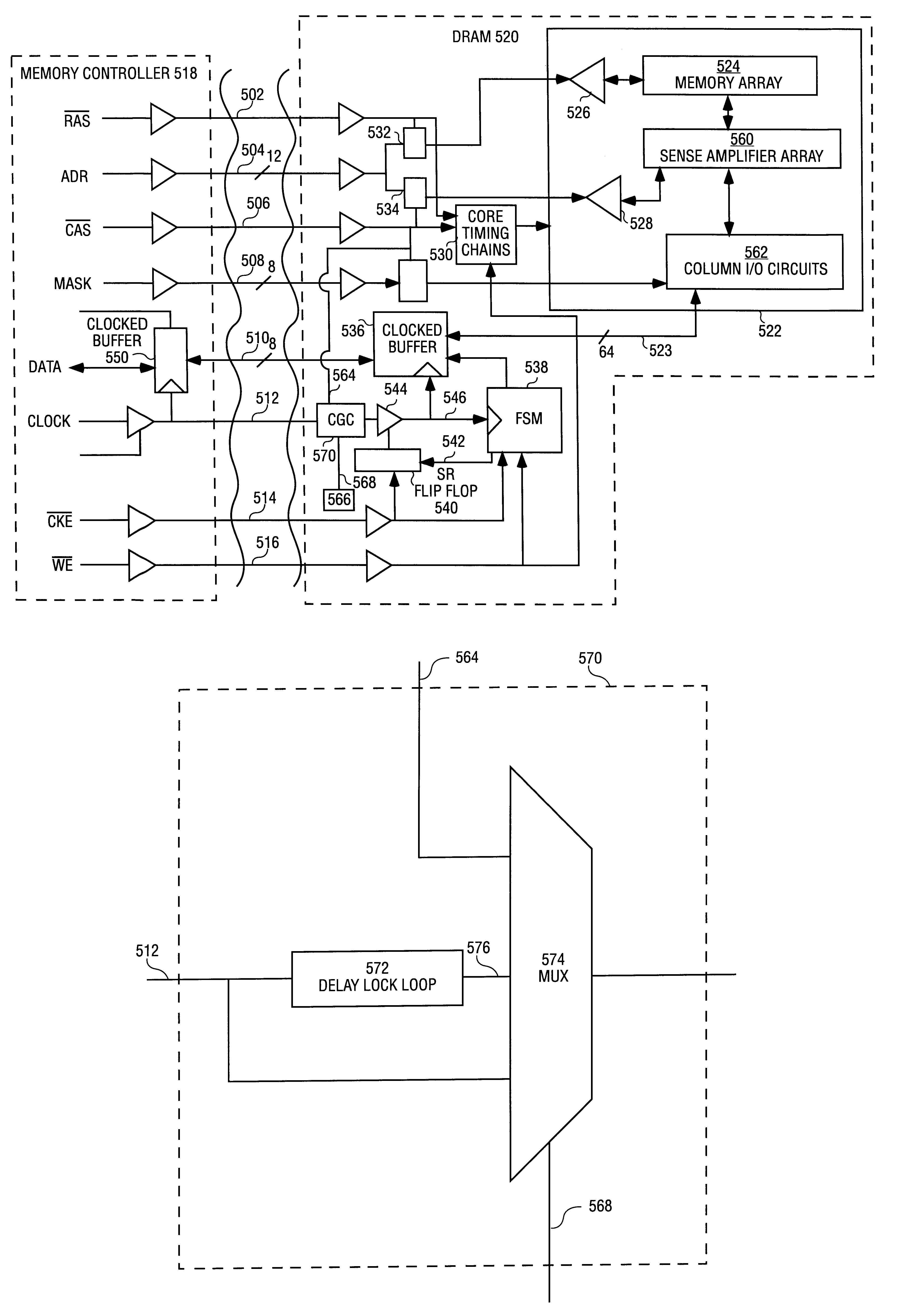
The internal clock signal is generated from an external clock signal that may selectively pass through a delay lock loop within the memory device. The memory device may support higher clock frequencies when the external clock signal passes through the delay lock loop to drive the data transfer circuits during a data transfer. Energy may be saved by circumventing the delay lock loop and using an external clock signal with a relatively slower frequency to drive the data transfer circuits during a data transfer.
In an alternate embodiment, DRAM 520 includes address transition detect circuitry, thus avoiding the need of separate CAS line 506 and signal. Address transition detect circuitry monitors the address bus 504 to detect transitions in the data that is being sent on the address bus 504. When a transition is detected, DRAM 520 restarts the timing chains 530 causing data corresponding to a new address to fall out of the column I / O circuits 562.
In an alternate embodiment, the WE signal can be sampled at the falling edge of CKE. To increase transmission bandwidth, the input receive path of DRAM 520 and the output transmit path of DRAM 520 can be separately compensated. For example, clock generation circuit 570 and clock buffer 544 may be replaced with two clock generation circuit / clock buffer combinations, where one clock generation circuit / clock buffer combination is used to drive clocked buffer 536 to receive data and a different clock generation circuit / clock buffer combination is used to drive clocked buffer 536 to transmit data. Power is saved by activating only the clock generation circuit / clock buffer combination that will be involved in the transfer. By sampling the WE signal at the falling edge of CKE, the DRAM has more time between when the type of transaction (read or write) is known and when the data transfer will begin. During this interval the DRAM activates the clock buffer that corresponds to the type of transaction to be performed.
Significantly, all of the steps performed up to step 816 are performed in an asynchronous manner. The use of an asynchronous mechanism to perform these steps reduces the latency between the fall of the RAS signal and the time that the appropriate row of data is sensed. By the time step 810 has been performed, the clock buffer 544 has been on long enough to provide a stable clock signal that may be used to synchronously transfer the data involved in the transaction.

Problems solved by technology

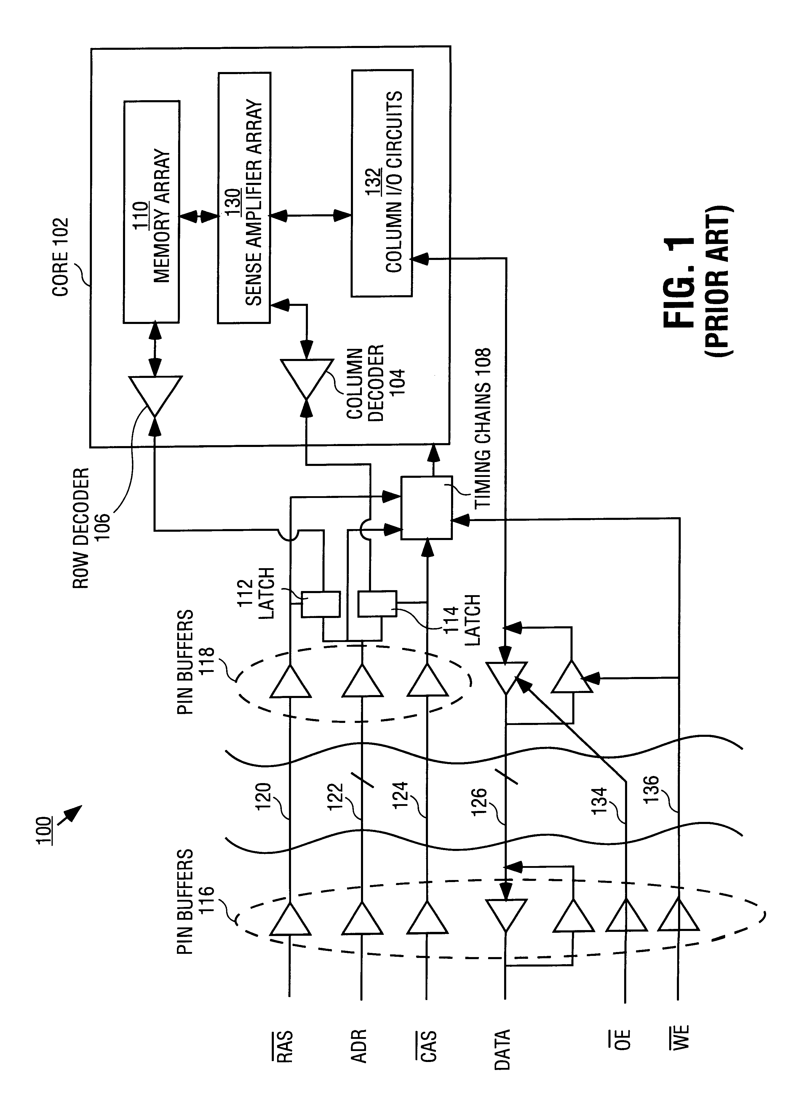
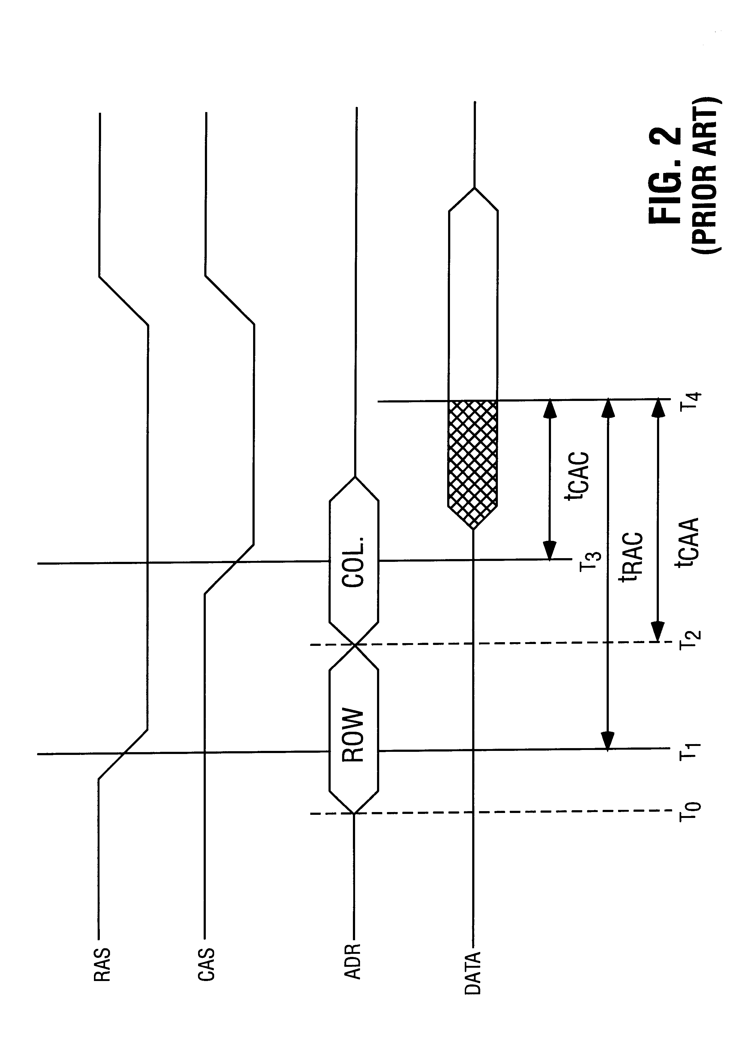
DRAMs built with an asynchronous RAS / CAS interface have difficulty meeting the high memory bandwidth demands of many current computer systems.
Because system 300 is synchronous, various issues arise that do not arise in asynchronous systems.
Unbalanced pipeline stages waste computational time.
Typically the execution time of each step is not substantially larger than the sum of these overheads, so the latency is significantly increased by them.
In addition, the architecture must take into account jitter that occurs when various data queues are clocked.
However, the higher rates are achieved at the expense of increased latency and power consumption.
Specifically, the time required to clock control and address data through various pipeline stages increases the delay between when an address for a read operation is transmitted and when the data from the specified address is actually supplied by the SDRAM.
Further, systems that use SDRAMs typically consume more power than the systems that use EDO DRAMs because, when the clock is enabled, the SDRAM interface is clocked whether or not a data transfer operation is actually being performed.
The time used to enable the clock signal further increases the delay between the time that data is desired and the time that the requested data is available.

Method used


Image

  • Asynchronous request/synchronous data dynamic random access memory
  • Asynchronous request/synchronous data dynamic random access memory
  • Asynchronous request/synchronous data dynamic random access memory

Examples


Embodiment Construction

In the embodiment illustrated in FIG. 5a, the throughput is maximized by providing separate lines for each type of signal so that the signals which are separated can function simultaneously. However, as a general rule, the higher the number of lines required by a memory system, the more expensive it is to manufacture the components for the memory system. Therefore, the approach shown in FIG. 5a may not be optimal when the cost of manufacturing is taken into account. In an alternative embodiment to that shown in FIG. 5a, the number of lines is reduced by multiplexing some of the lines to allow the same lines to carry more than one type of signal.

According to an alternative embodiment, the mask signal can be sent over the address bus 504, eliminating the need for mask lines 508. FIG. 9 is a timing diagram illustrating the timing of the signals generated during a write operation in such an embodiment. The timing proceeds in the same fashion as described above with reference to FIG. 7 w...


PUM


Abstract

A method and system for transferring information within a computer system is provided. The system includes a memory device that has a lower power mode in which data transfer circuitry is not driven by a clock signal, and a higher power mode in which data transfer circuitry is driven by a clock signal. The system further includes a memory controller that sends control signals to the memory device to initiate a data transfer transaction. The memory device receives the control signals asynchronously, and assumes the second mode in response to one of the control signals. While the memory device is in the second mode, the memory controller sends a control signal to identify a particular clock cycle. The memory device synchronously transfers the data. The memory device determines when to begin the data transfer based on the identified clock cycle and the type of data transfer that has been specified.

Description

The present invention relates to digital storage devices, and more specifically, to dynamic random access memory.Improvements in fabrication technology have resulted in dynamic random access memories (DRAMs) with increased density, faster performance, and higher operating frequencies. Because overall memory bandwidth requirements are rising and the number of DRAMs in a system is falling, the ability to quickly transport data to and from each DRAM has become increasingly important.ASYNCHRONOUS DRAMSIn conventional memory systems, the communication between a memory controller and DRAMs is performed through asynchronous communications. For example, the memory controller uses control signals to indicate to the DRAM when requests for data transactions are sent. The data transfers themselves are also performed asynchronously. To meet increased speed requirements, various enhanced asynchronous memory systems have been developed. One such system is the Extended Data Out (EDO) DRAM memory sy...

Claims


Application Information

Patent Timeline
IPC IPC(8): G11C7/10G06F12/00G06F13/16G11C5/00G11C7/22G11C8/18
CPCG06F13/16G11C7/1045G11C7/1051G11C7/1066G11C7/22G11C7/222G11C8/18G11C7/1072Y02B60/1228Y02D10/00
Inventor BARTH, RICHARD MAURICEHOROWITZ, MARK ALANHAMPEL, CRAIG EDWARDWARE, FREDERICK ABBOT
Owner RAMBUS INC
Learn More