Ferroelectric memory device

a ferroelectric capacitor and memory device technology, applied in the direction of information storage, static storage, digital storage, etc., can solve the problems of data storage in ferroelectric capacitors connected with sub-bitlines, data storage in ferroelectric capacitors cannot be increased, and interconnect potential may be changed,

Inactive Publication Date: 2006-01-10
SEIKO EPSON CORP
View PDF9 Cites 46 Cited by
  • Summary
  • Abstract
  • Description
  • Claims
  • Application Information

AI Technical Summary

Benefits of technology

[0009]The present invention may provide a noise-resistant ferroelectric memory device while hierarchizing bitlines and / or wordlines without causing sub-bitlines and / or sub-wordlines connected with unselected memory cells to be in a floating state.
[0023]The sub-bitlines in the selected block are connected to the main bitlines through the first sub-bitline select switches, and the sub-bitlines in the unselected blocks are connected to the common potential supply line through the second sub-bitline select switches. This prevents all the sub-bitlines in the selected and unselected blocks from floating, whereby the influence of disturbance noise can be reduced.
[0024]In a ferroelectric memory device according to another aspect of the present invention, the wordlines are hierarchized instead of the bitlines. Each main wordline is connected to one end of a sub-wordline through a first sub-wordline select switch, and a common potential supply line is connected to the other end of the sub-wordline through a second sub-wordline select switch in the same manner as described above. The sub-wordlines are prevented from floating by complementarily turning on the first and second sub-wordline select switches during memory access. Therefore, the influence of disturbance noise can be reduced.
[0025]According to yet another aspect of the present invention, both the bitlines and the wordlines are hierarchized. In the unselected block, the sub-bitlines are connected to the second common potential supply line through the second sub-bitline select switches, and the sub-wordlines are connected to the first common potential supply line through the second sub-wordline select switches. This prevents the sub-bitlines and the sub-wordlines from floating. Therefore, since the common potential is applied to both ends of each memory cell in the unselected block, the potential difference becomes 0 V, whereby the nonvolatile state can be maintained without being influenced by disturbance noise.
[0027]The common potential may be supplied to the sub-bitlines and / or the sub-wordlines of all the memory cells during a standby period in which no block is selected. In this case, the common potential may be substantially the same as a bitline potential and / or a wordline potential during the standby period. This enables the voltage applied to all the memory cells to be set at 0 V during the standby period. These potentials may be set to be substantially the same as the potential of the common potential supply line during an operation period, in the standby period after turning the power on. This enables charge / discharge current of each line to be reduced when transitioning from the standby period to the operation period, whereby the transitioning time can be reduced.

Problems solved by technology

However, since the active ferroelectric memory device has a large memory area in comparison with a flash memory or EEPROM which is known as a nonvolatile memory device in which a memory cell is formed by one element, the capacity cannot be increased.
In this case, the interconnect potential may be changed if noise is applied from the outside, whereby data stored in the ferroelectric capacitors connected with the sub-bitline may be destroyed.

Method used


Image

  • Ferroelectric memory device
  • Ferroelectric memory device
  • Ferroelectric memory device

Examples


first embodiment

1. First Embodiment

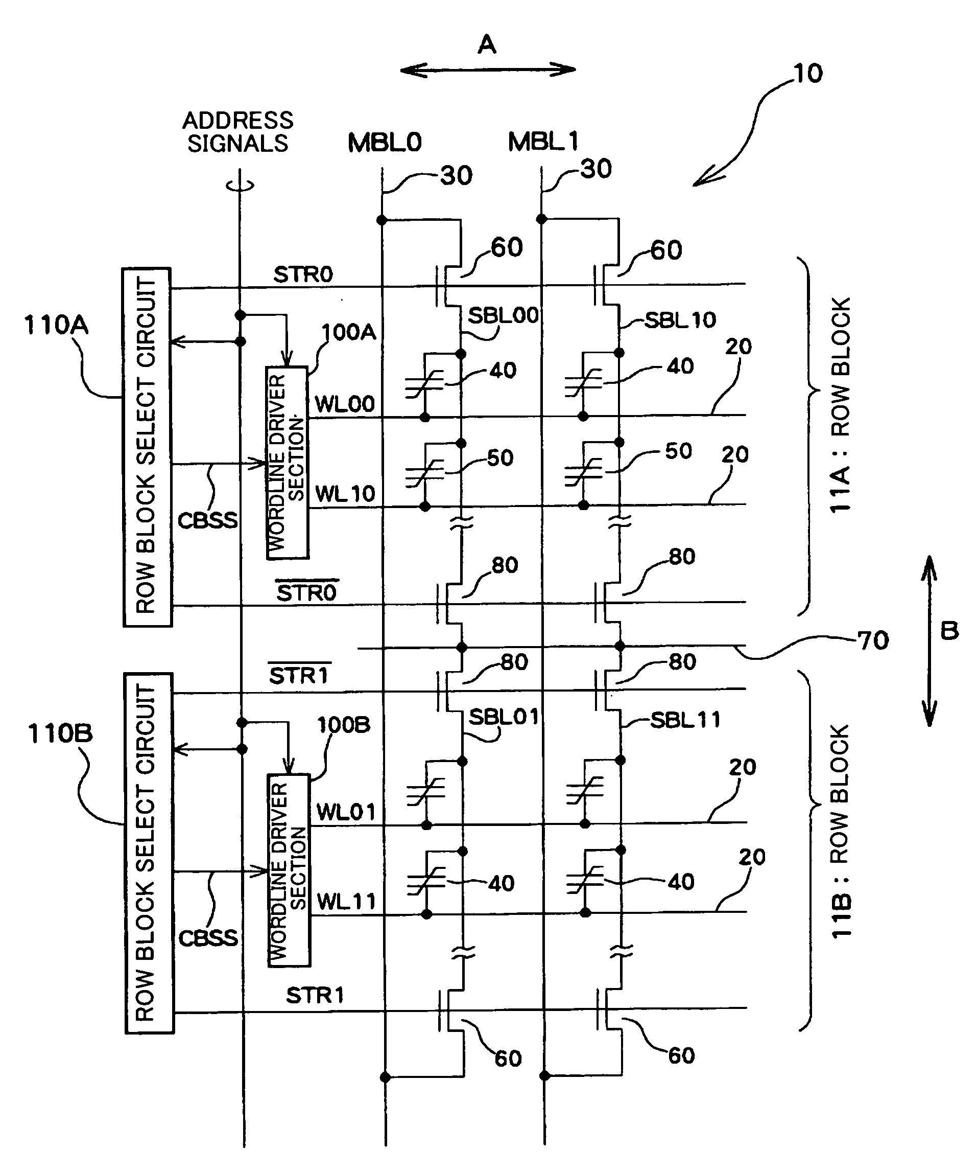
[0037]FIG. 1 shows a first embodiment of the present invention. In a memory cell array region 10 shown in FIG. 1, a row direction A in which wordlines 20 extend is defined as a first direction, and a column direction B in which hierarchized main bitlines 30 and sub-bitlines 40 extend is defined as a second direction. However, the present invention is not limited thereto. The memory cell array region 10 shown in FIG. 1 is divided into a plurality of row blocks 11A, 11B, . . . at least in the column direction B.

[0038]Wordline driver sections 100A and 100B and row block select circuits 110A and 110B are provided corresponding to the row blocks 11A and 11B, respectively.

[0039]The memory cell array region 10 is described below. In the present embodiment, the bitlines are hierarchized. Specifically, the sub-bitline 40 is provided for each of the main bitlines 30 in each of the row blocks 11A and 11B. In the row block 11A, the sub-bitline SBL00 is provided for the main b...

second embodiment

2. Second Embodiment

[0059]In a memory cell array region 200 shown in FIG. 6, a row direction A in which hierarchized main wordlines 210 and sub-wordlines 220 extend is defined as a first direction, and a column direction B in which bitlines 230 extend is defined as a second direction. However, the present invention is not limited thereto. The memory cell array region 200 shown in FIG. 6 is divided into a plurality of column blocks 201A, 201B, . . . at least in the row direction A.

[0060]Bitline driver sections 300A and 300B and block select circuits 310A and 310B are provided corresponding to the column blocks 201A and 201B, respectively.

[0061]In the present embodiment, the wordlines are hierarchized. Specifically, the sub-wordline 220 is provided for each of the main wordlines 210 in each of the column blocks 201A and 201B. In the column block 201A, the sub-wordline SWL00 is provided for the main wordline MWL0, and the sub-wordline SWL10 is provided for the main wordline MWL1. In th...

third embodiment

3. Third Embodiment

[0070]The configuration shown in FIG. 8 is the first embodiment shown in FIG. 1 combined with the second embodiment shown in FIG. 6. In FIG. 8, components having the same function as the components in FIGS. 1 and 6 are denoted by the same reference numbers.

[0071]In a memory cell array region 400 shown in FIG. 8, a row block 411 is formed in units of the sub-bitlines 40 subordinate to the main bitlines 30, and a column block 412 is formed in units of the sub-wordlines 220 subordinate to the main wordlines 210.

[0072]As is clear from the first and second embodiments, in the third embodiment in which the first and second embodiments are combined, the sub-bitline 40 and the sub-wordline 220 connected with the unselected memory cell in the unselected block can be set at the common potential (Vs / 3) through the first and the second common potential supply lines 70 and 250 without causing the sub-bitline 40 and the sub-wordline 220 to float. Therefore, the potential differ...


PUM


Abstract

A ferroelectric memory device including a memory cell array region having reduced influence of disturbance noise and divided into row blocks for every sub-bitline subordinate to main bitlines. One end of each sub bitline is connected to the main bitline through a first sub bitline select switch. The other end of the sub bitline is connected to a common potential supply line through a second sub-bitline select switch which is turned on complementarily with the first sub-bitline select switch.

Description

[0001]Japanese Patent Application No. 2003-10153 filed on Jan. 17, 2003, is hereby incorporated by reference in its entirety.BACKGROUND OF THE INVENTION[0002]The present invention relates to a ferroelectric memory device.[0003]As a ferroelectric memory device, an active ferroelectric memory device including 1T / 1C cells in which one transistor and one capacitor (ferroelectric) are disposed in each memory cell, or including 2T / 2C cells in which a reference cell is further disposed in each memory cell, has been known.[0004]However, since the active ferroelectric memory device has a large memory area in comparison with a flash memory or EEPROM which is known as a nonvolatile memory device in which a memory cell is formed by one element, the capacity cannot be increased.[0005]A ferroelectric memory device in which each memory cell is formed by one ferroelectric capacitor is known (Japanese Patent Application Laid-open No. 9-116107). Japanese Patent Application Laid-open No. 9-116107 disc...

Claims


Application Information

Patent Timeline
Patent Type & Authority Patents(United States)
IPC IPC(8): G11C11/22G11C7/18
CPCG11C7/18G11C11/22G11C2211/4013G11C2029/2602
Inventor YAMAMURA, MITSUHIRO
Owner SEIKO EPSON CORP
Why Eureka
Try Eureka