Nonvolatile semiconductor storage apparatus having reduced variance in resistance values of each of the storage states

a technology of nonvolatile semiconductors and storage apparatuses, which is applied in the direction of static storage, digital storage, instruments, etc., can solve the problems of large variance in the state of memory cells, the difference in source-drain potential of mos transistors, and the variation of threshold voltages

Active Publication Date: 2006-01-10
SHARP KK
View PDF3 Cites 39 Cited by
  • Summary
  • Abstract
  • Description
  • Claims
  • Application Information

AI Technical Summary

Benefits of technology

[0033]According to one aspect of the present invention, there is provided a nonvolatile semiconductor storage apparatus comprising: a first memory cell capable of storing a plurality of data values; a second memory cell capable of storing a plurality of data values; a resistance regulation section capable of regulating resistance, which regulates resistance such that a difference between a resistance value of a first connection line connected to the first memory cell and a resistance value of a second connection line connected to the second memory cell is reduced.
[0049]According to the present invention, a resistance regulation section reduces a difference in cumulative resistance values of connection lines, connected to a plurality of memory cells, at each of memory cells. Thus, it is possible to prevent the memory cells from not being properly accessed due to a difference in cumulative resistance values of connection lines connected to the memory cells at each of the memory cells.
[0050]Furthermore, at at least one of an end of a source line and an end of a bit line, a resistance value corresponding to a position of a memory cell in accordance with an address signal designating an address of the memory cells is added to at least one of source line resistance values and bit line resistance values at each of the memory cells, which are varied depending on the positions of the memory cells, so that the sum total of path resistances is balanced. Thus, it is possible to suppress a variance in storage states of the memory cells.
[0052]Thus, the invention described herein makes possible the advantages of providing a nonvolatile semiconductor storage apparatus which can prevent data stored in a memory cell from not being properly accessed during an access to a memory cell such as a write operation, erase operation, read operation and the like to a memory cell.

Problems solved by technology

Such a difference in the cumulative resistance values of the source line at memory cells causes problems such as differences in source-drain potentials of the MOS transistors and a variation in threshold voltages (ON resistances).
Such a variance in the memory cell states may be a big problem particularly when a multi-level technique is introduced so that a memory cell can store three or more data values.
Thus, incorrect data may be obtained.
Thus, it is not easy to suppress a variance in cumulative resistance values of the source line at each of the memory cells in accordance with the positions of the memory cells.

Method used


Image

  • Nonvolatile semiconductor storage apparatus having reduced variance in resistance values of each of the storage states
  • Nonvolatile semiconductor storage apparatus having reduced variance in resistance values of each of the storage states
  • Nonvolatile semiconductor storage apparatus having reduced variance in resistance values of each of the storage states

Examples


example 1

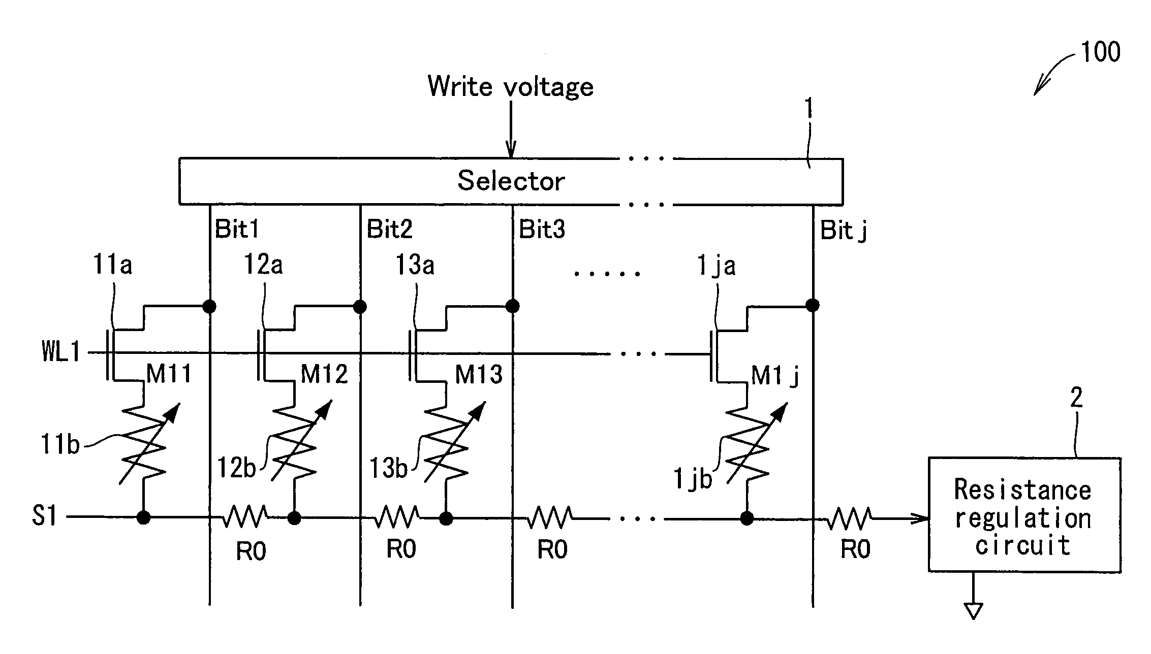
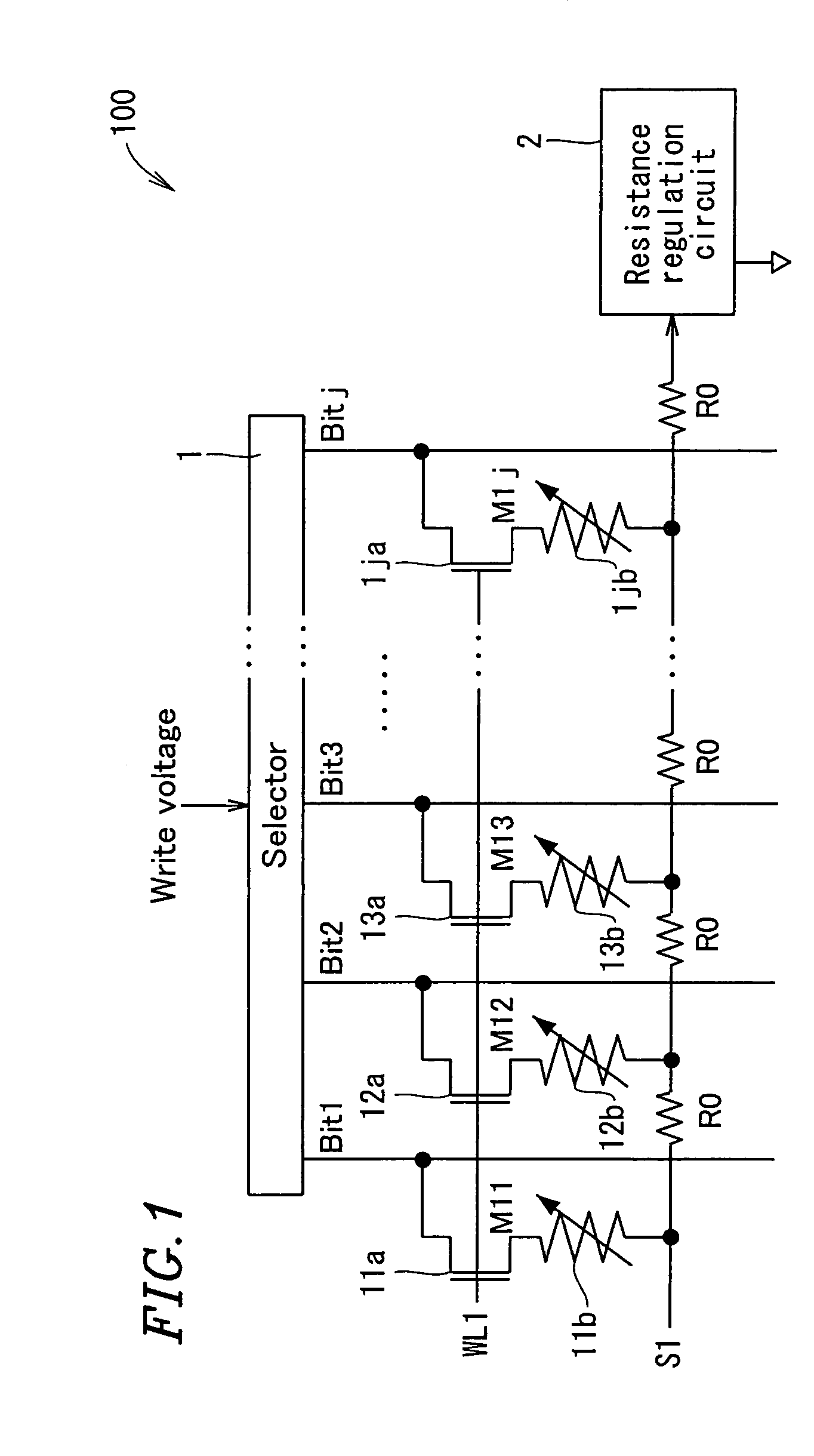
[0065]FIG. 1 is a circuit diagram showing one line of an important part of a nonvolatile semiconductor storage apparatus 100 according to Example 1 of the present invention.

[0066]The nonvolatile semiconductor storage apparatus 100 comprises a memory array including a plurality of memory cells M11 through Mnj (n and j are natural numbers) arranged in a matrix. Each of the memory cells M11 through Mnj is a 1T1R memory using a variable resistance element and a current control element.

[0067]FIG. 1 illustrates one line (one row) of the memory cells M11 through M1j in the memory array. The memory cell is now described in more detail by considering one of the memory cells M11 through M1j, for example, a memory cell M11. The memory cell M11 includes an n-type MOS transistor 11a which acts as a current control element (also referred to as a selection transistor) and a variable resistance element 11b of which the resistance is varied by an electric pulse (a material thereof includes, for exam...

example 2

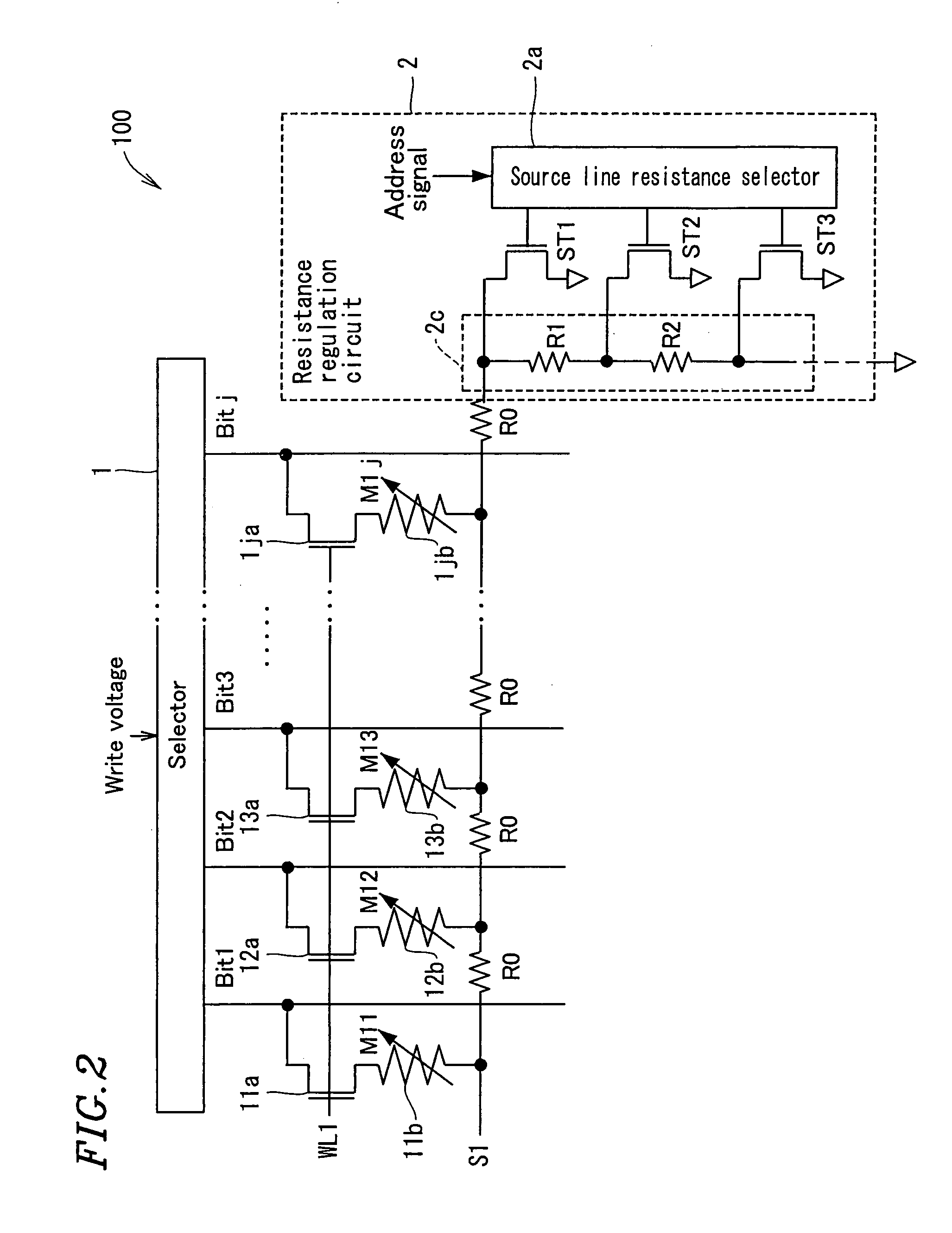
[0106]In Example 1, a resistance regulation circuit is provided at a terminal end side of a source line. In Example 2, a resistance regulation circuit is provided before start portions of bit lines.

[0107]FIG. 4 is a circuit diagram showing one line of an important part in a nonvolatile semiconductor storage apparatus 200 according to Example 2 of the present invention.

[0108]As the nonvolatile semiconductor storage apparatus described with reference to Example 1, the nonvolatile semiconductor storage apparatus 200 comprises a memory array including a plurality of memory cells M11 through Mnj (n and j are natural numbers) arranged in a matrix. Each of the memory cells M11 through Mnj is a 1T1R memory using a variable resistance element and a current control element.

[0109]FIG. 4 illustrates one line (one row) of memory cells M11 through M1j in a memory array. The memory cell is described in more detail with respect to one of the memory cells M11 through M1j, for example, a memory cell ...


PUM


Abstract

A nonvolatile semiconductor storage apparatus including: a first memory cell capable of storing a plurality of data values; a second memory cell capable of storing a plurality of data values; a resistance regulation section capable of regulating resistance, which regulates resistance such that a difference between a resistance value of a first connection line connected to the first memory cell and a resistance value of a second connection line connected to the second memory cell is reduced.

Description

BACKGROUND OF THE INVENTION[0001]1. Field of the Invention[0002]The present invention relates to a nonvolatile semiconductor storage apparatus.[0003]2. Description of the Related Art[0004]One known nonvolatile semiconductor storage apparatus is a floating-gate type flash memory. Data is written to a floating-gate type flash memory by injecting charges to a floating gate to change a threshold voltage of a MOS transistor.[0005]FIG. 7 is a circuit diagram showing an important part of a conventional floating-gate type flash memory 700.[0006]In the flash memory 700, a plurality of memory cells M111 through M11j are arranged within a matrix. Each memory cell includes a MOS transistor having a floating gate. In the flash memory 700, a plurality of word lines and a plurality of source lines oriented along a row direction are alternately located and a plurality of bit lines are oriented along a column direction.[0007]In order to simplify the description, FIG. 7 shows j memory cells M111 thro...

Claims


Application Information

Patent Timeline
Patent Type & Authority Patents(United States)
IPC IPC(8): G11C11/00G11C5/06G11C11/56G11C11/15G11C13/00G11C16/04
CPCG11C5/063G11C11/5685G11C13/0023G11C13/0069G11C13/0007G11C11/16G11C2213/79G11C2213/31G11C16/04
Inventor MATSUOKA, NOBUAKI
Owner SHARP KK
Why Eureka
Try Eureka