Liquid crystal display device

a liquid crystal display and display device technology, applied in non-linear optics, instruments, optics, etc., can solve the problems of reducing the efficiency of light utilization, limiting scaling development, and thicker conventional backlight modules with fluorescent lamp sources, so as to reduce the weight and thickness of the liquid crystal display device, and enhance light utilization efficiency.

Active Publication Date: 2006-01-17
HANNSTAR DISPLAY CORPORATION
View PDF22 Cites 67 Cited by
  • Summary
  • Abstract
  • Description
  • Claims
  • Application Information

AI Technical Summary

Benefits of technology

[0011]Another object of the present invention is to provide an integrated liquid crystal display device with better light utilization efficiency and thinner thickness.
[0016]The present invention improves on the prior art in that the liquid crystal display device is a fully integrated combination of the liquid crystal device and the OLED element serving as a backlight source. The structure invention greatly reduces light leakage caused by gaps, thereby enhancing light utilization efficiency. In addition, the liquid crystal device and the OLED element use the same substrate (the first substrate), thus the weight and thickness of the liquid crystal display device can be decreased. Moreover, since the OLED element of the liquid crystal display device of the invention can be a multi-color display, the present invention does not require color filter(s), thereby enhancing light utilization efficiency and ameliorating the disadvantages of the prior art.

Problems solved by technology

Conventional backlight modules with fluorescent lamp sources are, however, thicker and limits scaling development.
Additionally, in conventional liquid crystal display devices, polarizers are adhered to the outside surfaces of the liquid crystal display panel and gaps may remain between the polarizers and the liquid crystal display panel.
The gaps allow light leakage, decreasing the light utilization efficiency of the liquid crystal display device.
Polarizers, however, only block about 50% of the light during light polarization and drastically reduce the light utilization efficiency of the liquid crystal display device.
Moreover, color filters only block about 66% of the light, thereby further reducing the light utilization efficiency.
The traditional LCD device has poor light utilization efficiency and scaling limitation problems.

Method used


Image

  • Liquid crystal display device
  • Liquid crystal display device
  • Liquid crystal display device

Examples


first embodiment

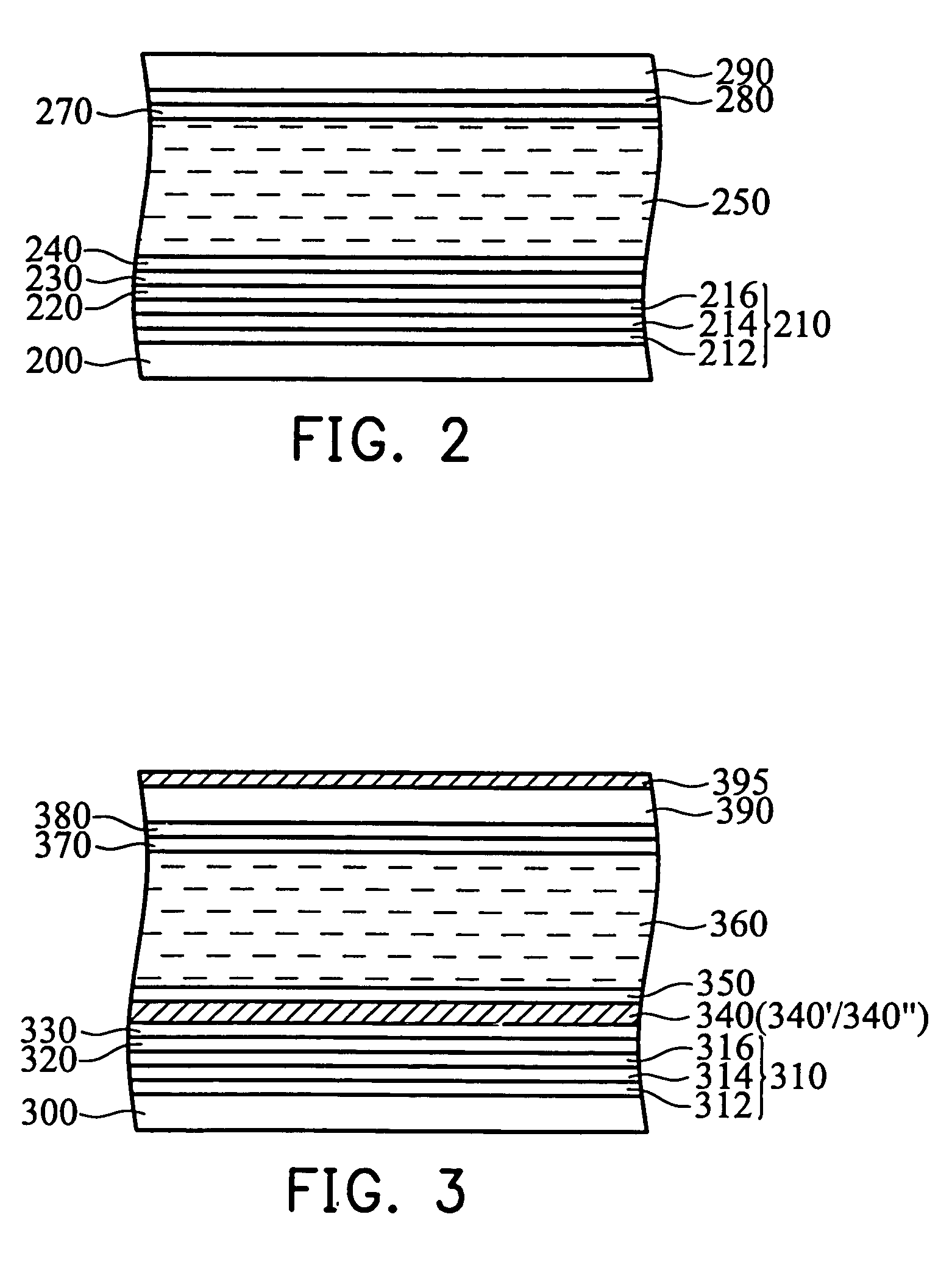
[0027]FIG. 2 is a sectional view of a liquid crystal display device according to a first embodiment of the present invention.

[0028]In FIG. 2, a first substrate 200 is provided. The first substrate 200 can be glass or flexible plastic and can be transparent or opaque.

[0029]In FIG. 2, an organic electroluminescent display (OLED) element 210 serving as a backlight source is formed on the first substrate 200. A method for forming the OLED element 210 follows, but is not intended to limit the OLED process and the OLED profile of the present invention. For example, a cathode 212 is formed on the first substrate 200. An organic emitter layer 214 is formed on the cathode 212. Then, an anode 216 is formed on the organic emitter layer 214. The cathode 212 is commonly a metal electrode, such as Mg—Ag alloy or Li—Al alloy. The organic emitter layer 214 can comprise doped polymers which can emit different colors of light (e.g. red, green, and blue). The anode 216 is a transparent electrode, such...

second embodiment

[0036]FIG. 3 is a sectional view of a liquid crystal display device according to a second embodiment of the present invention.

[0037]In FIG. 3, a first substrate 300 is provided. The first substrate 300 can be glass or flexible plastic and can be transparent or opaque.

[0038]An organic electroluminescent display (OLED) element 310 serving as a backlight source is formed on the first substrate 300. As a method for forming the OLED element 310 follows, but is not intended to limit the OLED process and the OLED profile of the present invention. For example, a cathode 312 is formed on the first substrate 300. An organic emitter layer 314 is formed on the cathode 312. Then, an anode 316 is formed on the organic emitter layer 314. The cathode 312 is commonly a metal electrode, such as Mg—Ag alloy or Li—Al alloy. The organic emitter layer 314 can comprise doped polymers which can emit different colors of light (e.g. red, green, andblue). The anode 316 is a transparent electrode, such as ITO ...

third embodiment

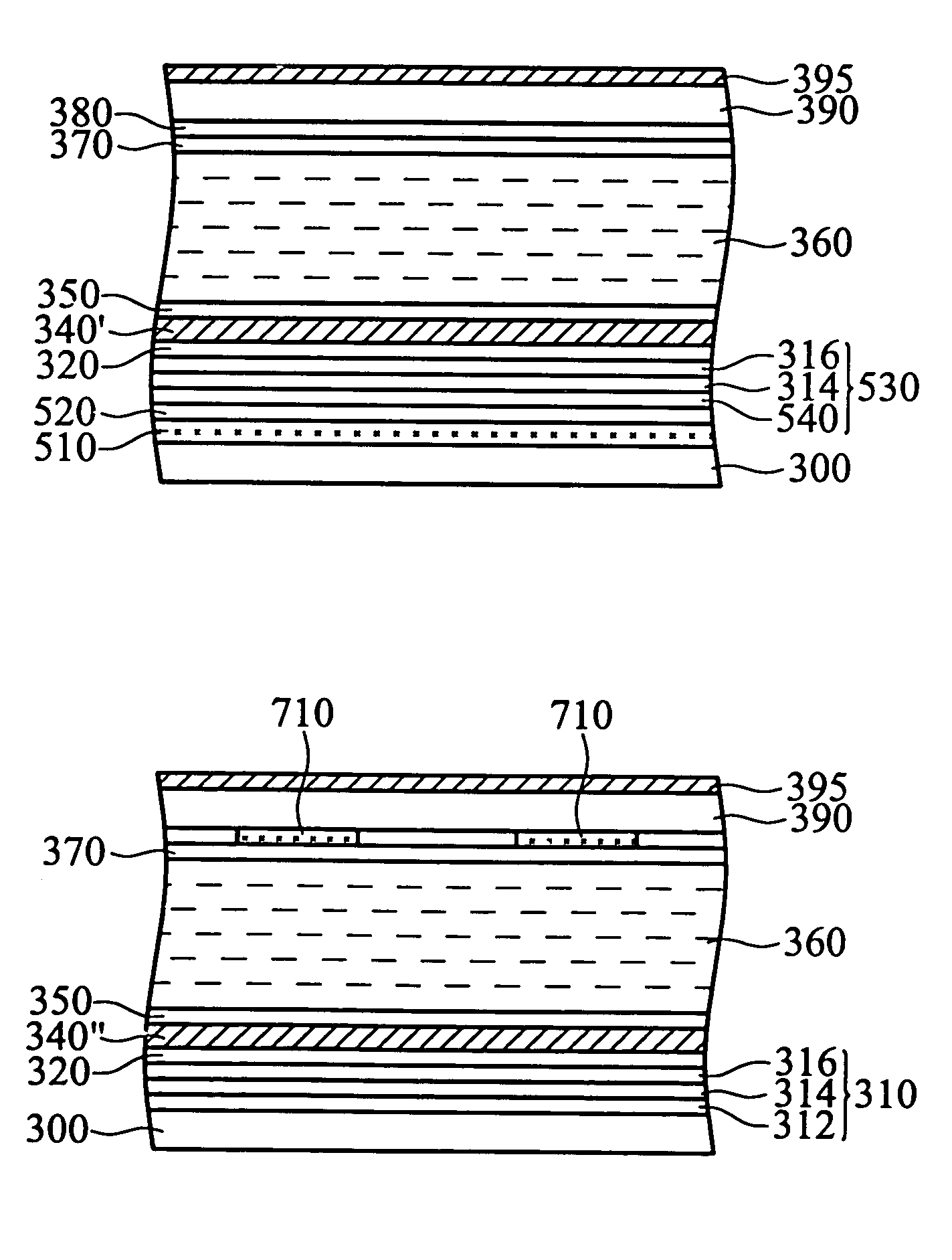
[0048]FIG. 5 is a sectional view of a liquid crystal display device according to a third embodiment of the present invention. Elements in FIG. 5 repeated from FIG. 3 use the same reference numbers. Additionally, because some materials and processes of the parts in the third embodiment are the same as the above, hence, their description is omitted. The difference between the third and second embodiments is that the LCD device of the third embodiment has a retardation film and a reflective layer disposed below the first polarizer (the reflective polarizer), thereby improving light utilization efficiency.

[0049]In FIG. 5, a first substrate 300 is provided. A reflective layer 510, such as aluminum, is formed on the first substrate 300. Then, a retardation film 520, such as a ¼λ retardation film, is formed on the reflective layer 510.

[0050]An organic electroluminescent display (OLED) element 530 serving as a backlight source is formed on the retardation film 520. The OLED element 530 comp...


PUM

PropertyMeasurementUnit
operating temperatureaaaaaaaaaa
transparentaaaaaaaaaa
voltageaaaaaaaaaa

Abstract

A liquid crystal display (LCD) device, with an organic electroluminescent display (OLED) element serving as a light source, a common electrode, and a polarizer which is a wire grid polarizer or a thin film polarizer are formed on a lower substrate. A pixel electrode is formed on an upper substrate. According to the invention, a thinner integrated LCD device with improved light utilization efficiency is obtained.

Description

BACKGROUND OF THE INVENTION[0001]1. Field of the Invention[0002]The present invention relates to a liquid crystal display (LCD) device, and more particularly, to an integrated liquid crystal display device having an organic electroluminescent display (OLED) element as a backlight source.[0003]2. Description of the Related Art[0004]A liquid crystal display (LCD) presents images by controlling the orientation of the liquid crystal molecules which in turn control the transmission of light. LCDs are frequently provided with a backlight module to enhance contrast and display visibility.[0005]Conventionally, in most liquid crystal display devices, the backlight module comprises fluorescent tubes arranged in parallel to a light guide plane, with a back reflector to enhance brightness, and a diffuser layer on the light guide plane to provide more uniform illumination to the liquid crystal device. In portable displays, for example, those used in mobile computers, small diameter cold cathode ...

Claims


Application Information

Patent Timeline
Patent Type & Authority Patents(United States)
IPC IPC(8): G02F1/1335G02F1/13357
CPCG02F1/133603G02F1/133528
Inventor YANG, KIE-HSIUNGCHEN, WEI-CHOU
Owner HANNSTAR DISPLAY CORPORATION
Why Eureka
Try Eureka