World line structure with single-sided partially recessed gate structure

a gate structure and world line technology, applied in the field of semiconductor devices, can solve the problems of device geometries continuing to decrease in size, the opening of the bit line, and the difficulty of fabricating conductive plugs connected to the bit lines and disposed between the word lines

Active Publication Date: 2006-01-31
NAN YA TECH
View PDF1 Cites 3 Cited by
  • Summary
  • Abstract
  • Description
  • Claims
  • Application Information

AI Technical Summary

Benefits of technology

[0013]Accordingly, an object of the present invention is to provide a novel word line structure with a single-sided partially recessed gate structure and the method for forming the same, which can prevent short circuit between the word line and the conductive plug connected to the bit line or prevent the bit line from opening due to poor electrical connection of the conductive plug.
[0014]Another object of the present invention is to provide a novel word line structure with a single-sided partially recessed gate structure and the method for forming the same, in which the single-sided partially recessed gate structure has a recess region near the bit line contact, instead of the conventional double-sided partially recessed gate structure, thereby preventing the contact resistance of the word line from increasing.

Problems solved by technology

The fabrication of conductive plugs connected to the bit lines and disposed between the word lines, however, becomes more difficult as memory device geometries continue to decrease in size.
Conversely, if the gate capping layer and the gate spacer of the word line are under etched during fabrication of the self-aligned bit line contact, the bit line contact may fail, resulting in an open circuit of the bit line after formation of the conductive plug with poor electrical connection.

Method used


Image

  • World line structure with single-sided partially recessed gate structure
  • World line structure with single-sided partially recessed gate structure
  • World line structure with single-sided partially recessed gate structure

Examples


Embodiment Construction

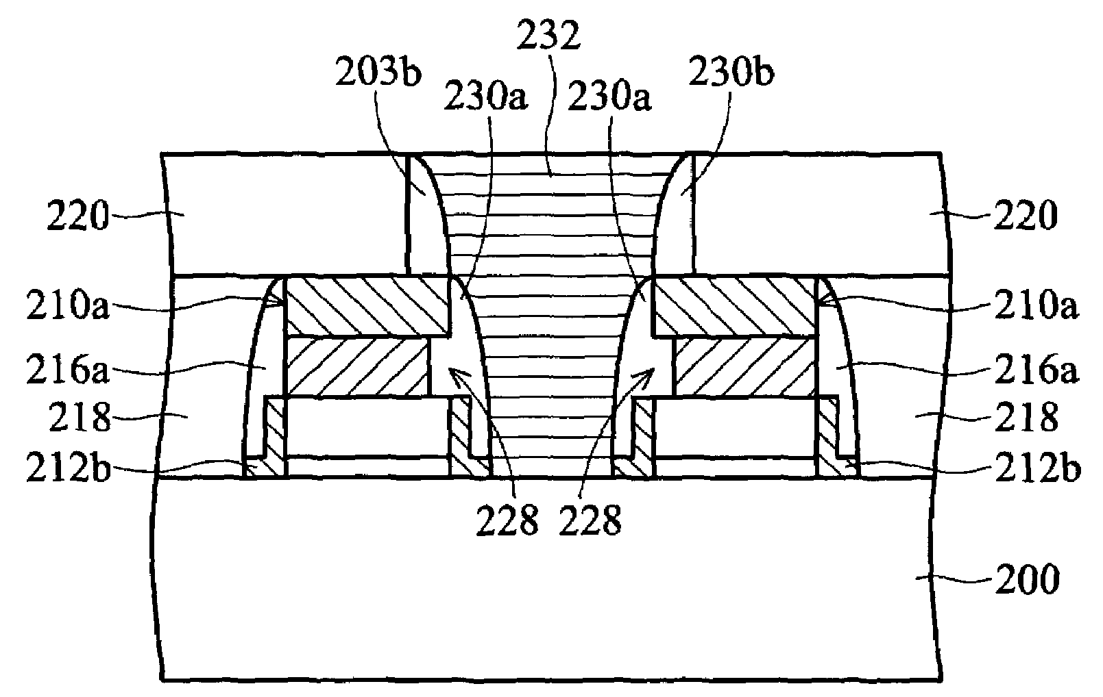
[0024]FIGS. 2a to 2g are cross-sections showing a method for forming a word line structure with a single-sided partially recessed gate structure for a semiconductor device, such as a DRAM.

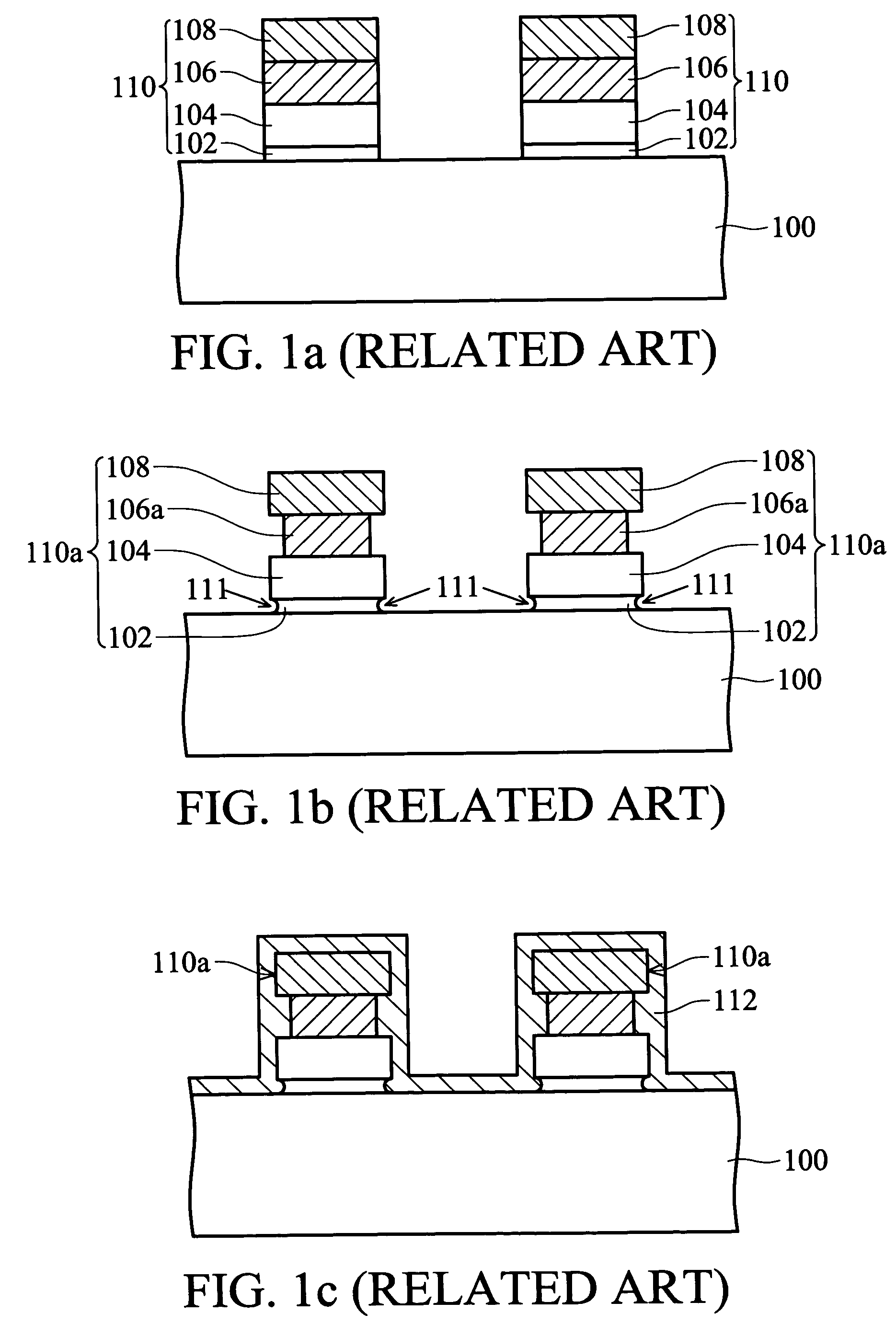
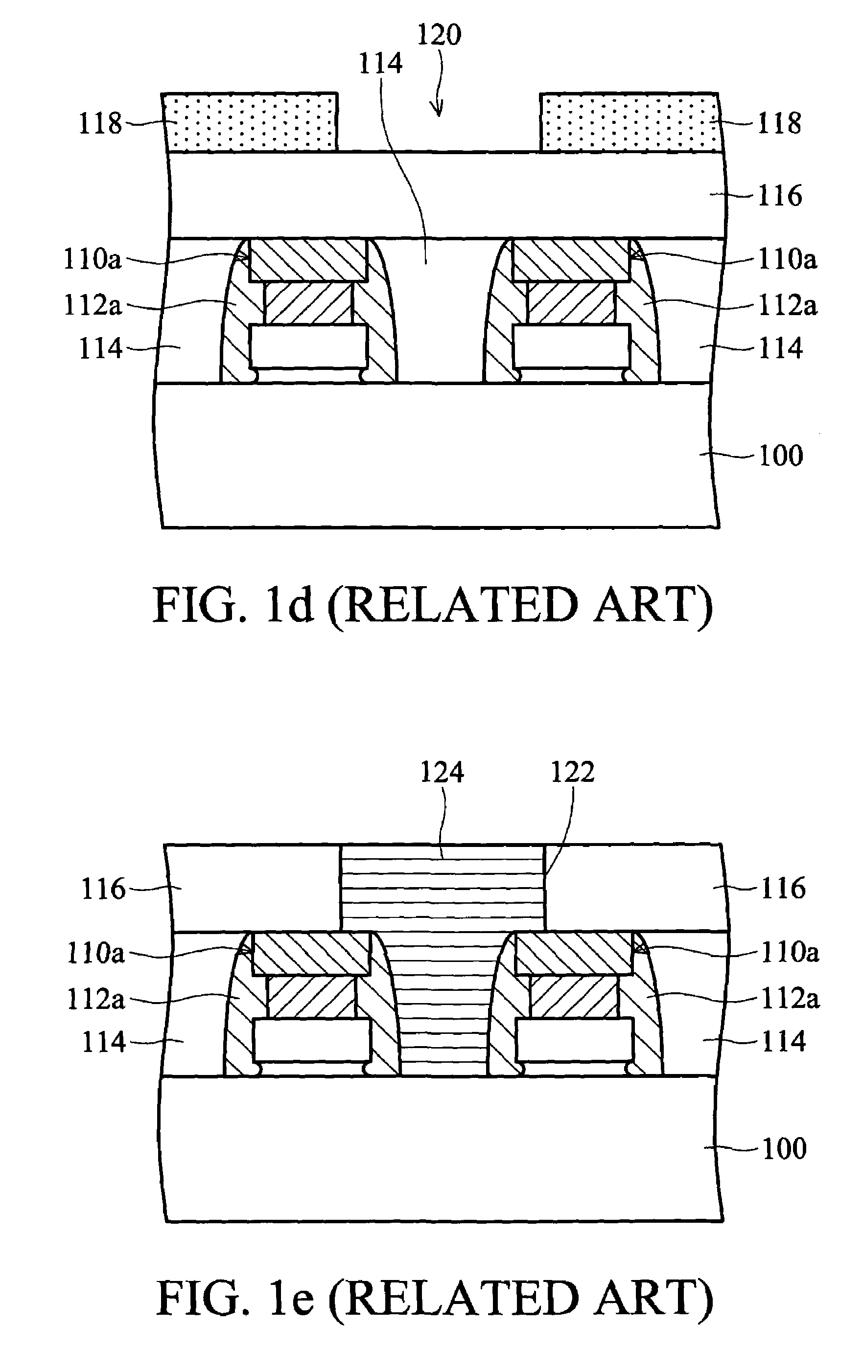
[0025]First, in FIG. 2a, a substrate 200, such as a silicon substrate, is provided. The substrate 200 may contain semiconductor devices, such as capacitors and resistors, used in the memory devices. Here, in order to simplify the diagram, only a flat substrate is depicted. Next, a dielectric layer 202, a first conductive layer 204, a second conductive layer 206, and a capping layer (not shown) are successively formed overlying the substrate 200.

[0026]In the invention, the dielectric layer 202 is used for definition of a gate dielectric layer, which can be a silicon oxide layer formed by thermal oxidation. Moreover, the first conductive layer 204 is used for definition of a gate electrode, which can be a polysilicon layer. The second conductive layer 206 is used as a portion of the gate electrode to...


PUM


Abstract

A word line structure with a single-sided partially recessed gate structure. The word line structure includes a gate structure, a first gate spacer, and a second gate spacer. The gate structure includes a gate dielectric layer, a first gate layer, a second gate layer, and a gate capping layer and has a recess region adjacent to one of opposing sidewalls of the second gate layer. The first gate spacer is disposed over opposing sidewalls of the gate dielectric layer and the first gate layer. The second gate spacer is disposed over opposing sidewalls of the gate structure and covers the first gate spacer. A method for forming a word line structure with a single-sided partially recessed gate structure is also disclosed.

Description

BACKGROUND OF THE INVENTION[0001]1. Field of the Invention[0002]The present invention relates in general to a semiconductor device, and more particularly, to a word line structure with a single-sided partially recessed gate structure.[0003]2. Description of the Related Art[0004]A dynamic random access memory (DRAM) is a common semiconductor memory device widely employed in electronic products. In order to increase the density of the memory devices and improve performance thereof, the size of memory devices must be reduced. The fabrication of conductive plugs connected to the bit lines and disposed between the word lines, however, becomes more difficult as memory device geometries continue to decrease in size. Therefore, many self-aligned processes have been developed for bit line contact fabrication, which are useful for the fabrication of the subsequent conductive plug. If the gate capping layer and the gate spacer of the word line are over etched during fabrication of the self-ali...

Claims


Application Information

Patent Timeline
Patent Type & Authority Patents(United States)
IPC IPC(8): H01L29/72H01L21/28H01L21/336H01L21/60H01L21/8242H01L29/423H01L29/76
CPCH01L21/76897H01L29/6656H01L27/10891H01L29/6653H01L27/10888H01L21/28114H01L27/10873H01L29/42376H10B12/05H10B12/488H10B12/485
Inventor KUAN, SHIH-FANWU, KUO-CHIEN
Owner NAN YA TECH
Why Eureka
Try Eureka