Uniform pressing apparatus

a pressing apparatus and uniform technology, applied in the field of uniform pressing apparatus, can solve the problems of poor design, degraded molding quality and manufacturing efficiency in mass production, and limited processing technology, and achieve good parallelism

Inactive Publication Date: 2006-02-07
IND TECH RES INST
View PDF5 Cites 40 Cited by
  • Summary
  • Abstract
  • Description
  • Claims
  • Application Information

AI Technical Summary

Benefits of technology

[0009]The primary objective of the present invention is to provide a uniform pressing apparatus applica

Problems solved by technology

However, this process is technically limited in the processing of features having a line width smaller than 100 nanometers due to the light diffraction.
Therefore, molding quality and manufacture efficiency in mass production are both degraded due to non-uniform distribution of imprinting pressure and poor parallelism between the mold and the substrate.
These problems often occurred as a result of poor designs or inferior processing/assembly of the imprint equipment, and apparently need to be resolved by improving the imprinting equipment
And with such apparatus design, there are too many modifications in terms of p

Method used


Image

  • Uniform pressing apparatus
  • Uniform pressing apparatus
  • Uniform pressing apparatus

Examples


first embodiment

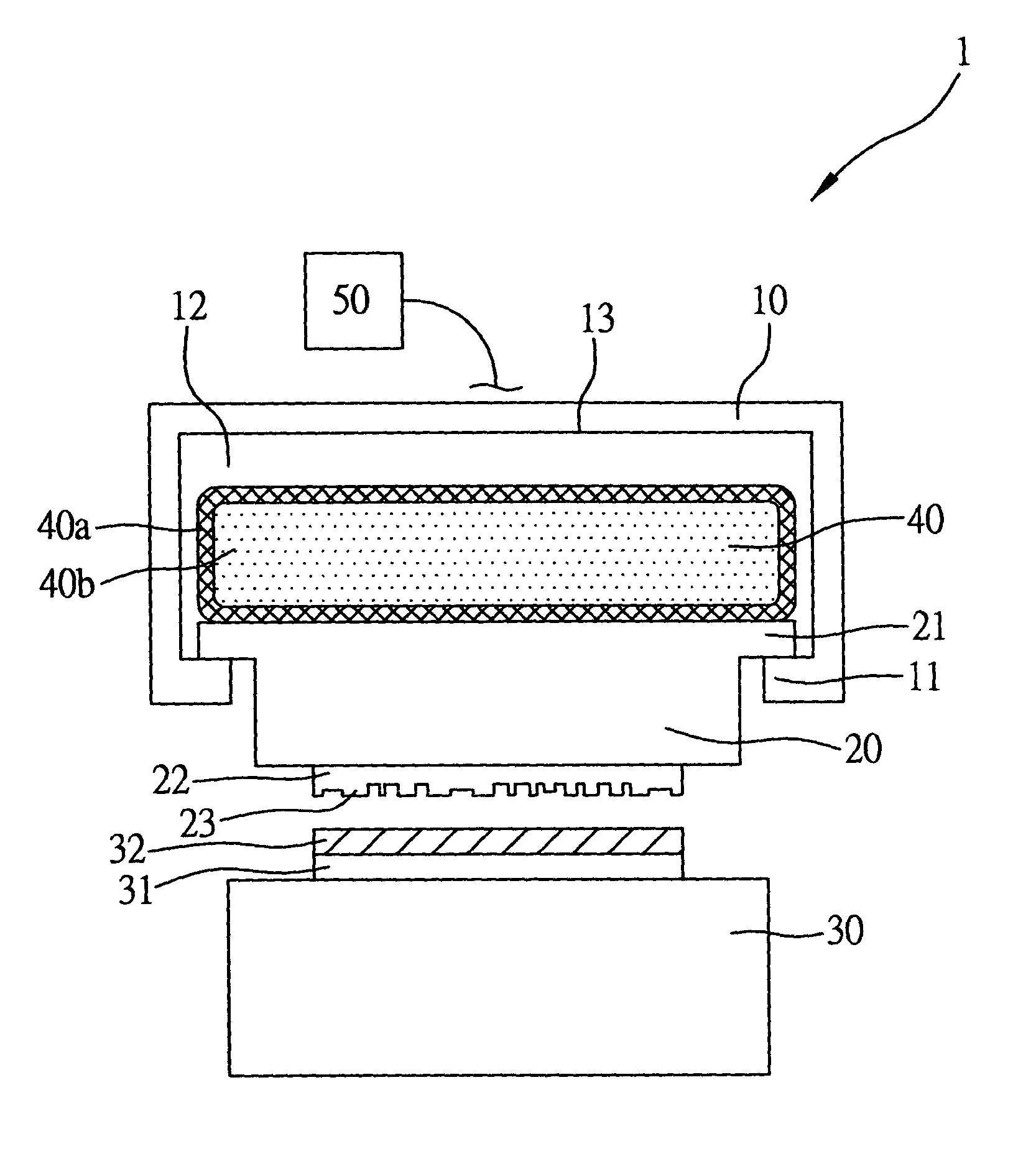
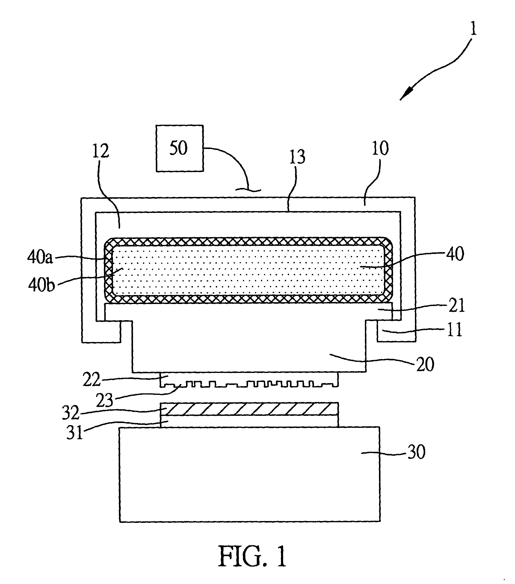
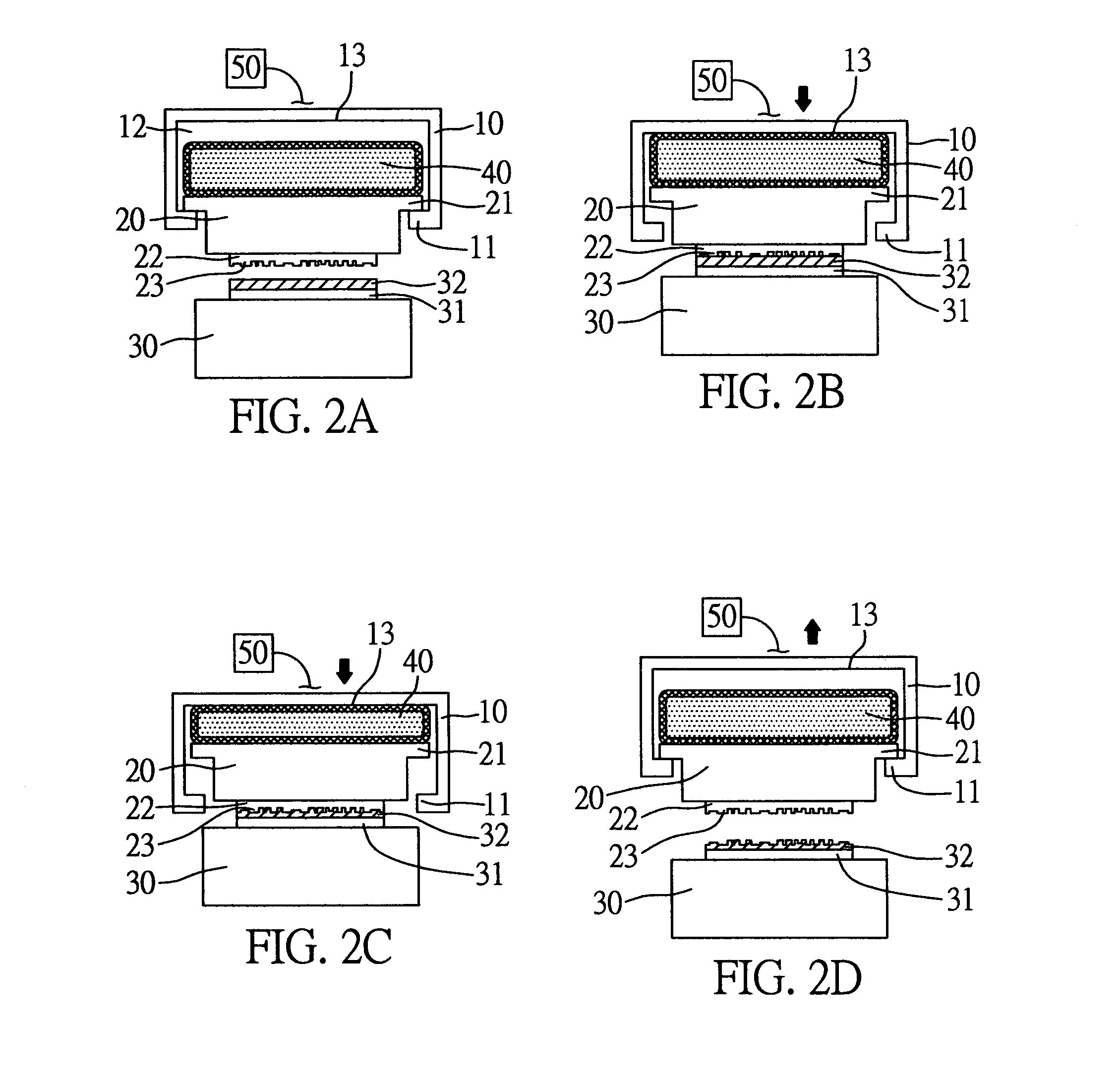
[0035]FIG. 2A through to FIG. 2D illustrate the operation of a uniform pressing apparatus according to the invention. Referring to FIG. 2A, a substrate 31 is subjected to a horizontal alignment with a mold 22. Referring to FIG. 2B, the power source 50 drives the housing 10, along with the first carrier unit 20 and the mold 22 to move toward the substrate 31 on the second carrier unit 30. Thereby, the nanoscale feature 23 on the mold 22 makes a contact with a moldable layer 32. Since the first flange 11 makes free contact with the second flange 21, the mold 22 and the substrate 31 are not restrained to each other when the mold 22 makes the contact with the substrate 31. Therefore, an optimal parallelism is achieved at the moment when the contact is made. As shown in FIG. 2B, the second flange 21 is detached from the first flange 11 as a result of a counteracting force that acts on the second flange 21 to push the second flange 21 away from the first flange 11. The housing 10 is still...

second embodiment

[0036]FIG. 3A through to FIG. 3D illustrate the operation of a uniform pressing apparatus according to the invention. Similarly, the invention includes a housing 10, a first carrier unit 20, a uniform pressing unit 40, a second carrier unit 40 and a power source 50. The power source 50 is mounted alongside the second carrier unit 30 to drive movement of the second carrier unit 30 towards the first carrier unit 20. The power source 50 further provides an imprint force, so that the imprinting process is carried out via the contact formed as a result of the substrate moving towards the nanoscale features. The substrate 31 is subjected to a horizontal alignment with the mold 22 as shown in FIG. 3A. The power source 50 drives the second carrier unit 30 and the substrate 31 on the second carrier unit 30 to move toward the first carrier unit 20 and the mold 22 on the first carrier unit 20, as shown in FIG. 3B. The first flange 11 makes a free contact with the second flange 21 to achieve op...

third embodiment

[0037]FIG. 4A through to FIG. 4D illustrate the operation of a uniform pressing apparatus according to the invention. Similarly, the invention includes a housing 10, a first carrier unit 20, a second carrier unit 30, a uniform pressing unit 40, and a power source 50. In this embodiment of the invention, the power source 50 includes a feeding power source 50a and an imprint power source 50b. The feeding power source 50a drives the housing 10 to move toward the second carrier unit 30, while the imprint power source 50b drives the uniform pressing unit 40 to exert pressure. The substrate 31 and the mold 22 are subjected to a horizontal alignment as shown in FIG. 4A. The feeding power source 50a drives the housing 10 to move downward along with the first carrier unit 20 and the mold 22. The first flange 11 makes the free contact with the second flange 21 to achieve optimal parallelism between the substrate 31 and the mold 22 when the substrate 31 makes the contact with the mold 22. Refe...


PUM

PropertyMeasurementUnit
Forceaaaaaaaaaa
Pressureaaaaaaaaaa
Electromagnetismaaaaaaaaaa

Abstract

A uniform pressing apparatus used in nanoimprint lithographic process is proposed, including a housing having a first flange; a first carrier unit for carrying an imprint mold and having at least one second flange freely attaches to the first flange; a second carrier unit for carrying a substrate; at least one uniform pressing unit mounted on a imprint force transmission path; and a power source driving at least one of the housing and the second carrier unit to allow a contact to be formed between the mold and the moldable layer. Therefore, the nanoimprint lithographic process is achieved with good parallelism between the substrate and the mold and with uniform pressure distribution.

Description

FIELD OF THE INVENTION[0001]The invention relates to a uniform pressing apparatus, and more particularly, to a uniform pressing apparatus which achieves good parallelism between a mold and a substrate via free contact of the mold and the substrate in nanoimprint lithography.BACKGROUND OF THE INVENTION[0002]In a conventional semiconductor process, a photolithographic process is usually used to form traces over a chip or a substrate. However, this process is technically limited in the processing of features having a line width smaller than 100 nanometers due to the light diffraction. Therefore, a nanoimprint lithographic (NIL) process is proposed to replace the photolithographic process for manufacturing devices with very high resolution, with a high throughput and a low manufacturing cost.[0003]FIG. 6A through to FIG. 6C illustrate the operation of a nanoimprint lithographic including a cycle of heating, imprinting, and cooling. At the heat stage as shown in FIG. 6A, a moldable layer...

Claims


Application Information

Patent Timeline
IPC IPC(8): B29C59/02
CPCB29C59/022Y10S425/019B29C2059/023
Inventor CHUNG, YONG-CHENLIN, CHIA-HUNGHSU, CHIA-CHUNCHEN, CHUAN-FENGFENG, WEN-HUNGCHEN, MING-CHI
Owner IND TECH RES INST
Why Eureka
Try Eureka