Signal channel configuration providing increased capacitance at a card edge connection

a technology of capacitance and signal channel, applied in the field of signal channel, can solve the problems of reducing signal quality and difficulty in achieving the proper impedance of high-speed signal channel

Inactive Publication Date: 2006-02-07
LENOVO (SINGAPORE) PTE LTD
View PDF12 Cites 51 Cited by
  • Summary
  • Abstract
  • Description
  • Claims
  • Application Information

AI Technical Summary

Problems solved by technology

It is often difficult to achieve a proper impedance for the a high-speed signal channel extending through such a connection because of the local inductance contributed by the contact terminal within the connector and because of the additional impedance associated with circuit traces adjacent the connector.
When effective compensation is not applied for these sources of inductance, discontinuities in the line impedance of the channel cause reflections that degrade signal quality.

Method used


Image

  • Signal channel configuration providing increased capacitance at a card edge connection
  • Signal channel configuration providing increased capacitance at a card edge connection

Examples


Embodiment Construction

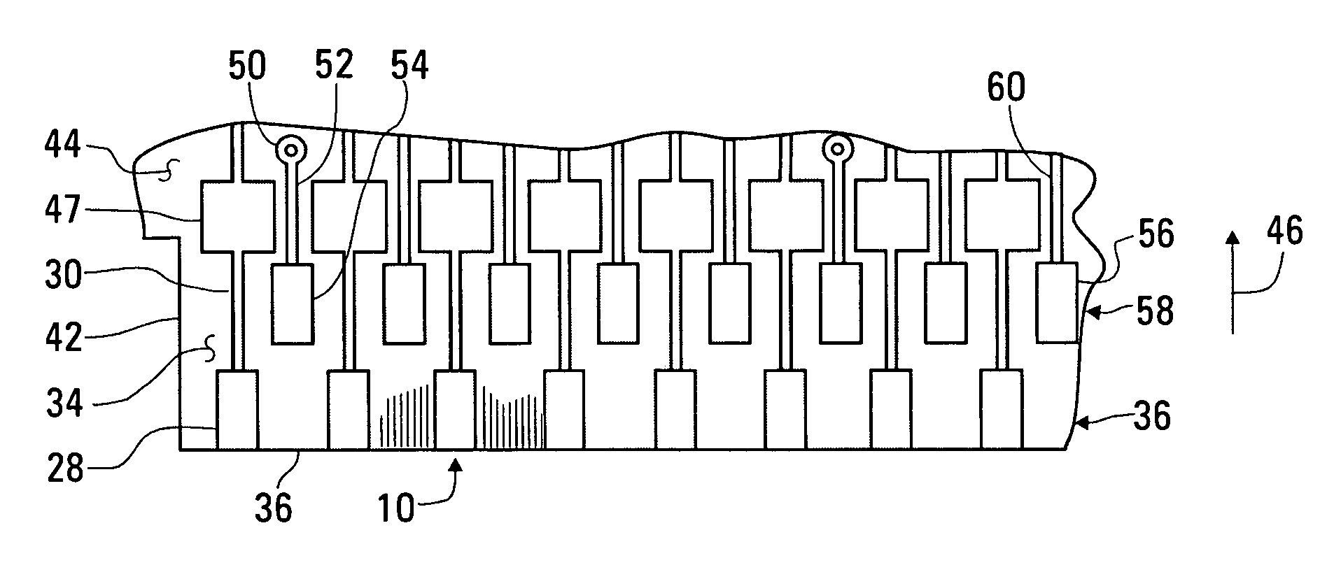
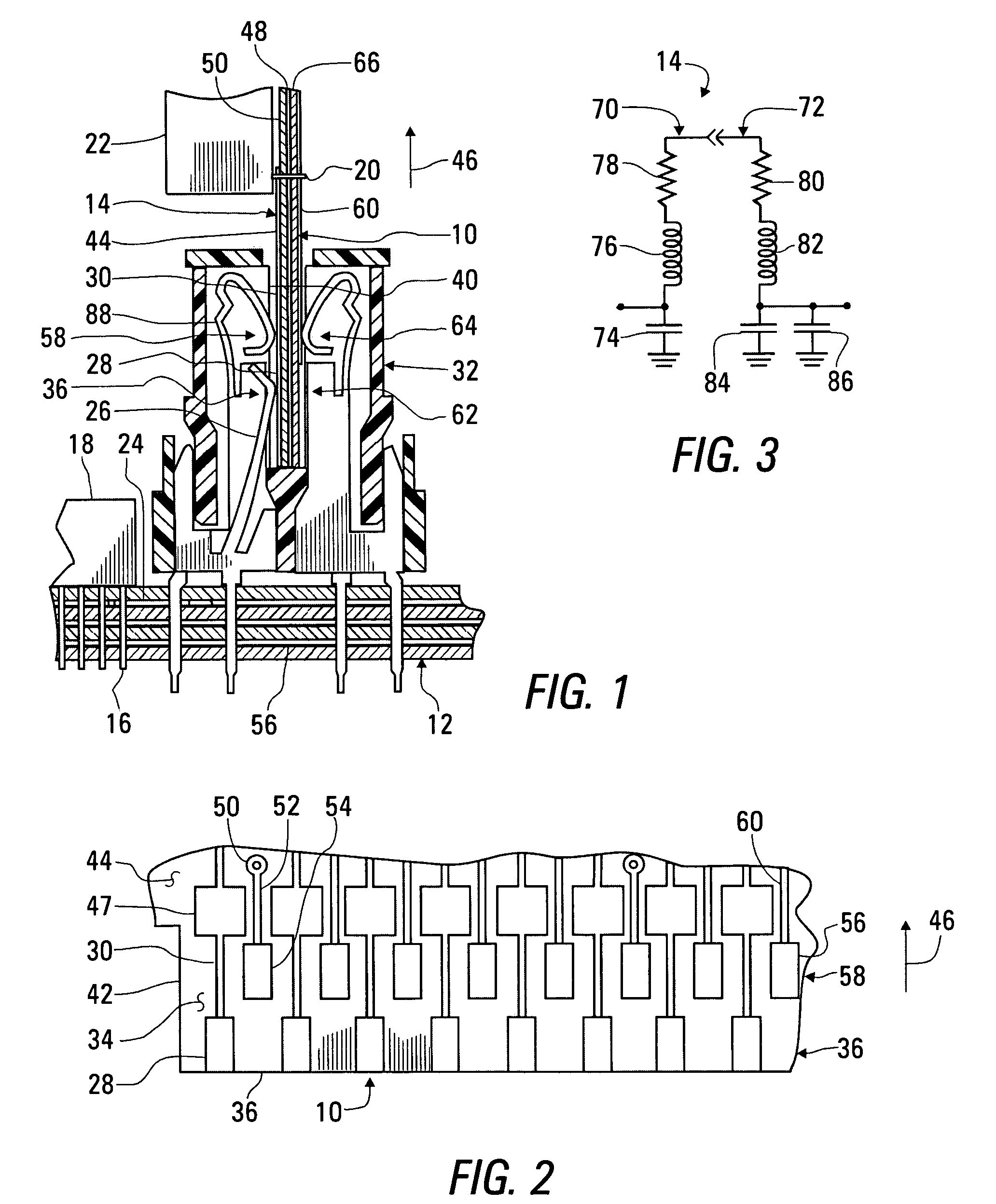
[0015]FIG. 1 is a fragmentary cross-sectional view of a daughter card 10, made in accordance with the invention, connected to a motherboard 12 to provide a number of signal channels 14 configured in accordance with the invention. Each of the signal channels 14 extends between a terminal 16 of a first device 18 on the motherboard 12 and a terminal 20 of a second device 22 on the daughter card 10. The signal channel 14 includes a board circuit trace 24, extending along the motherboard 12 between the terminal 16 of the first device 18, a first contact terminal 26, electrically connected to the board circuit trace 24, a first contact pad 28, contacted by the first contact terminal 26, and a first card circuit trace 30, extending along the daughter card 10 to an electrical connection with the terminal 20 of the second device 22. The first contact terminal 26 forms a part of a connector 32 attached to the motherboard 12. The devices 18, 22 are understood to be electronic devices that gene...


PUM


Abstract

A signal channel extends from motherboard to a daughter card across an edge connection. The daughter card includes a conductive plane that is held at a constant electrical potential. In order to compensate for a number of sources of inductance within the signal line at the edge connection, a circuit trace forming a portion of the signal channel includes an enlarged portion, spaced inward along the daughter card from the contact pads forming the edge connection, that adds capacitive coupling of the signal channel with the conductive plane.

Description

BACKGROUND OF THE INVENTION[0001]1. Field of the Invention[0002]This invention relates to a signal channel extending between an electronic device on a motherboard and an electronic device on a daughter card through a card edge connection, and, more particularly to a signal channel configuration having increased capacitance to electrical ground at the card edge connection to compensate for inductance introduced within a contact terminal forming part of the signal channel.[0003]2. Description of the Related Art[0004]Electrical connections are typically made between a motherboard and a daughter card through a card edge connection, with a number of contact pads extending in one or more rows along the edge of the daughter card being electrically connected to a similar number of contact terminals within a connector attached to the motherboard. It is often difficult to achieve a proper impedance for the a high-speed signal channel extending through such a connection because of the local in...

Claims


Application Information

Patent Timeline
Patent Type & Authority Patents(United States)
IPC IPC(8): H01R12/20H01R12/71H01R12/00H05K1/11H05K1/16
CPCH05K1/117H05K1/162Y10S439/951H05K2201/09672H05K2201/0792
Inventor AMINI, KAMRANDIEPENBROCK, JOSEPH CURTISEVANS, ROBERT JOSEPHSCOLLARD, MICHAEL LEO
Owner LENOVO (SINGAPORE) PTE LTD
Why Eureka
Try Eureka