Connector for memory card
a technology for connecting devices and memory cards, applied in the direction of coupling device connections, engagement/disengagement of coupling parts, instruments, etc., can solve the problems of the connector for memory cards becomes tough with respect to static electricity and external noise, and the deformation and abrasion of the housing rarely occur, etc., to achieve the effect of sufficient mechanical strength, easy grounding, and low cos
- Summary
- Abstract
- Description
- Claims
- Application Information
AI Technical Summary
Benefits of technology
Problems solved by technology
Method used
Image
Examples
first embodiment
[0116]A first embodiment of the present invention is described with reference to the drawings.
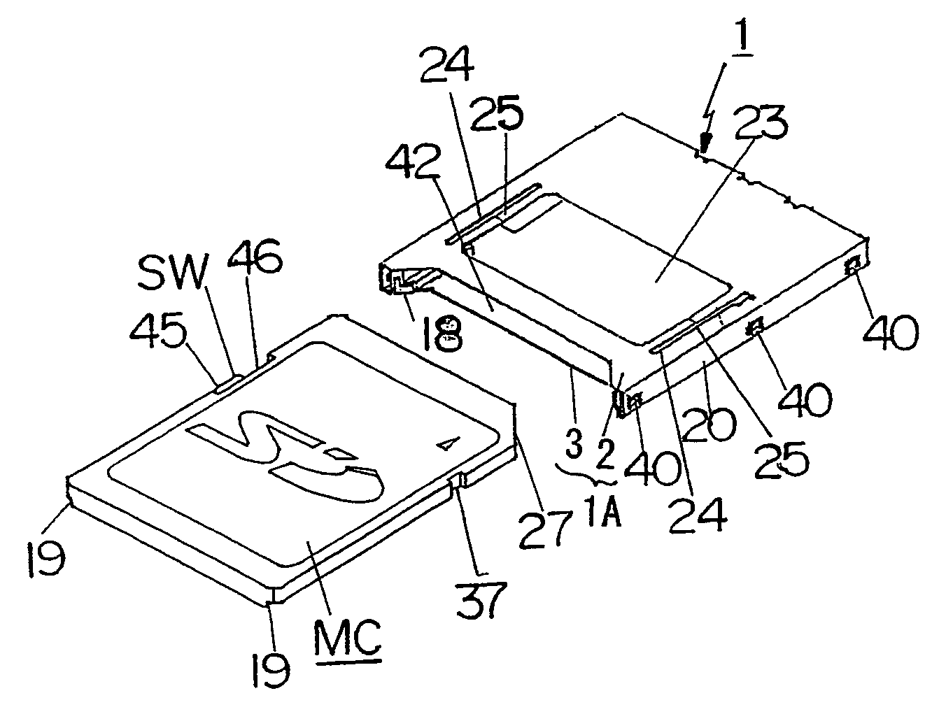
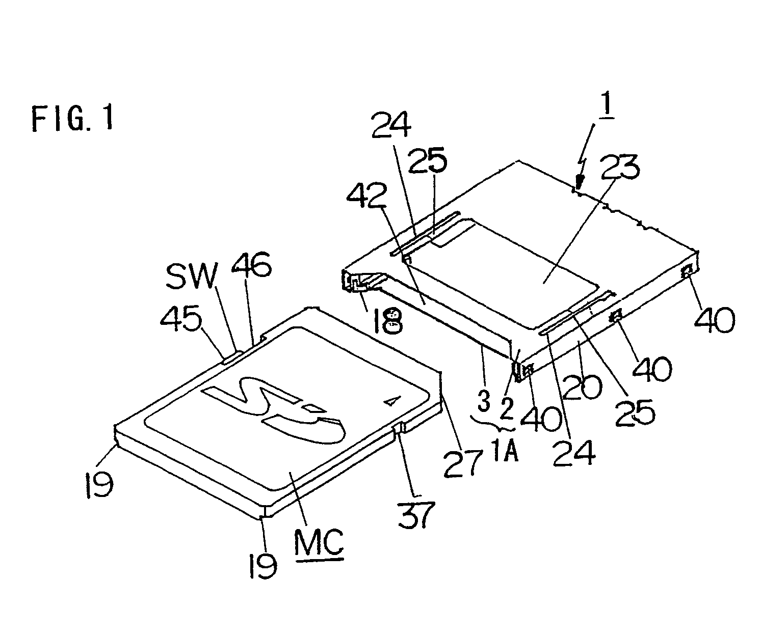
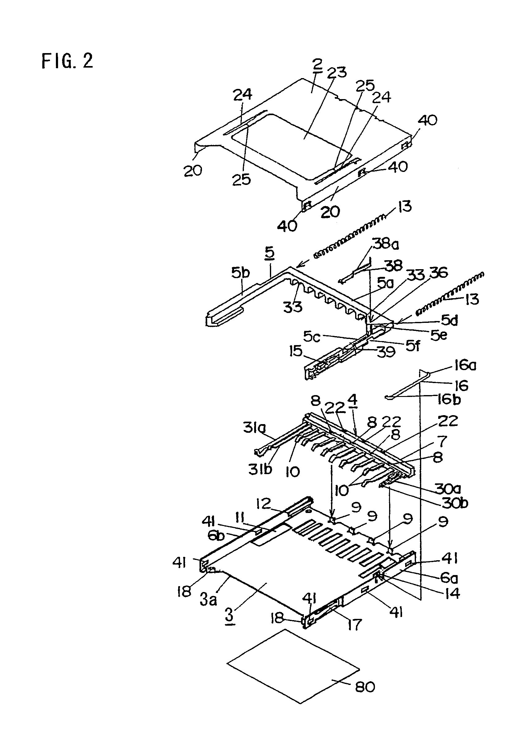
[0117]FIG. 1 shows appearances of a memory card such as an SD card designated by a symbol “MC” and a connecter 1 in the first embodiment. FIG. 2 shows a configuration of the connector 1.
[0118]As can be seen from FIGS. 1 and 2, a planiform housing 1A of the connector 1 is configured by a cover shell 2 and a base shell 3, and the housing 1A has an opening 42 formed on a front face through which the memory card MC is inserted into the housing 1A. The cover shell 2 is formed by punching a thin stainless steel plate to a predetermined shape, and bending the punched plate (blank). Similarly, the base shell 3 is formed by punching a thin stainless steel plate to a predetermined shape, and bending the punched plate (blank). The housing 1A is assembled by engaging the cover shell 2 with the base shell 3. A contact block 4 is provided at a position in the vicinity of a rear end in the housing 1A. A s...
second embodiment
[0177]A second embodiment of the present invention is described. The connector 1 in the first embodiment is on condition that the base shell 3 is fixed on the circuit substrate. Alternatively, in the second embodiment, the cover shell 2 is to be fixed on the circuit substrate. The connector 1 in the second embodiment is called reverse type.
[0178]Details of the reverse type base shell 3 in the second embodiment are shown in FIGS. 14A to 14D. FIG. 14A shows a rear view of the base shell 3. FIG. 14B shows a plan view of the base shell 3. FIG. 14C shows a front view of the base shell 3. FIG. 14D shows a side view of the base shell 3.
[0179]In comparison with FIGS. 3A to 3D in the first embodiment, it is found that the soldering portions 61 are upwardly bent on the front end of the base shell 3. The height of the soldering portions 61 is a little higher than the thickness of the housing 1A in a manner so that the soldering portions 61 is positioned above the outer face of the top plate of...
third embodiment
[0186]A third embodiment of the present invention is described. In the description of the third embodiment, the elements which are substantially the same as those in the first embodiment are not referred, and the characteristic elements in the third embodiment are mainly described.
[0187]FIG. 19 shows a configuration of the connector 1 in the third embodiment. In comparison with FIG. 2 in the first embodiment, a pair of spring guide members 100 are independently formed from the base shell 3. The coil springs 13 are fitted into the cuttings 47 formed on the both sides of the base member 7 of the contact block 4 and the grooves 35a and 35b formed on the arms 5b and 5c of the slider 5 from openings on the rear face of the housing 1A. Subsequently, the spring guide members 100 are engaged with the housing 1A in a manner so that spring guide rods 101 of the spring guide members 100 are fitted into the inner hollows of the coil springs 13. Cuttings 110 are formed on the rear end portion of...
PUM
 Abstract
Description
Claims
Application Information


