Flat panel display device and manufacturing method thereof

a flat panel display and construction technology, applied in static indicating devices, dielectric characteristics, instruments, etc., can solve the problems of difficult to absorb such stress, peeling stress in the connecting portion between the display panel and the tcp, and the whole panel substrate becomes defective, so as to reduce the number of assembly steps, prevent the connection, and reduce the load on the tcp

Inactive Publication Date: 2006-02-07
GOLD CHARM LTD
View PDF9 Cites 23 Cited by
  • Summary
  • Abstract
  • Description
  • Claims
  • Application Information

AI Technical Summary

Benefits of technology

[0021]In view of the state of art mentioned above, an object of the present invention is to provide a flat panel display device having a connecting construction of each of TCP's, whose length is limited to a necessary minimum to reduce a size of a rounded portion thereof to thereby make thickness and size thereof possible to further reduce and a method for manufacturing the same flat panel display device.
[0022]The present invention is achieved on the basis of not a mere construction required by the rounded portions of the TCP's after the display device is completed. That is, the inventors of the present invention have studied the mechanism of stress generation in a TCP in the bending step of a slit of the TCP to form a rounded portion slit and found that a peel-off stress not only during an assembling operation of the display device but also after the completion of the display device can be relaxed without requiring an extra length of the TCP by newly providing an auxiliary slit in the TCP, which is bent during the assembling operation and returns to a flat state after the display device is completed. The present invention is achieved on the basis of the above-mentioned discovery.
[0024]That is, the TCP employed in the present invention includes not only an easily deformable region, which is easily bent and provided for the rounded portion, but also the auxiliary slit, which is temporarily bent. The slit for rounded portion will be referred to as “main slit” and the auxiliary slit will be referred to as “sub slit”.
[0036]In the present invention having such features, the load exerted on the TCP is absorbed by not only the main slit region but also the sub slit region, which is temporarily bent during the assembling operation. Therefore, when the liquid crystal panel or the circuit substrate moves on the chassis, it is possible to reduce the load exerted on the TCP by the main and sub slits. Consequently, it is possible to prevent the connection between the liquid crystal panel and the circuit substrates from being broken during the mounting of the circuit substrate and the circuit in the TCP from being broken during a vibration test or a shock test of the liquid crystal display device. Furthermore, according to the present invention, it is possible to reduce the number of assembling steps of the liquid crystal display device and the number of parts thereof to be assembled.

Problems solved by technology

Particularly, reduction of an area of the liquid crystal display device except an image display region thereof, that is, a frame portion of the liquid crystal display device, and reduction of thickness of the liquid crystal display device itself are important problems to be solved.
However, if the driver LSI directly formed on the display panel substrate is defective, the whole panel substrate becomes defective.
Further, a peeling stress is generated in the connecting portion between the display panel and the TCP when the latter is pulled up.
On the other hand, since, when the size of liquid crystal display panel is increased, the liquid crystal display panel may be deformed due to thermal expansion of the panel itself, the adhesive is usually not used to fix the liquid crystal panel to the chassis.
It is difficult to absorb such stress by only the slit provided in only the rounded portion of each TCP.
The above-mentioned problems may also occur in other flat panel type display devices.

Method used


Image

  • Flat panel display device and manufacturing method thereof
  • Flat panel display device and manufacturing method thereof
  • Flat panel display device and manufacturing method thereof

Examples


first embodiment

[0050]a flat display device of the present invention will be described with reference to FIGS. 2 to 6 in which the same or equivalent portions are depicted by the same reference numerals, respectively.

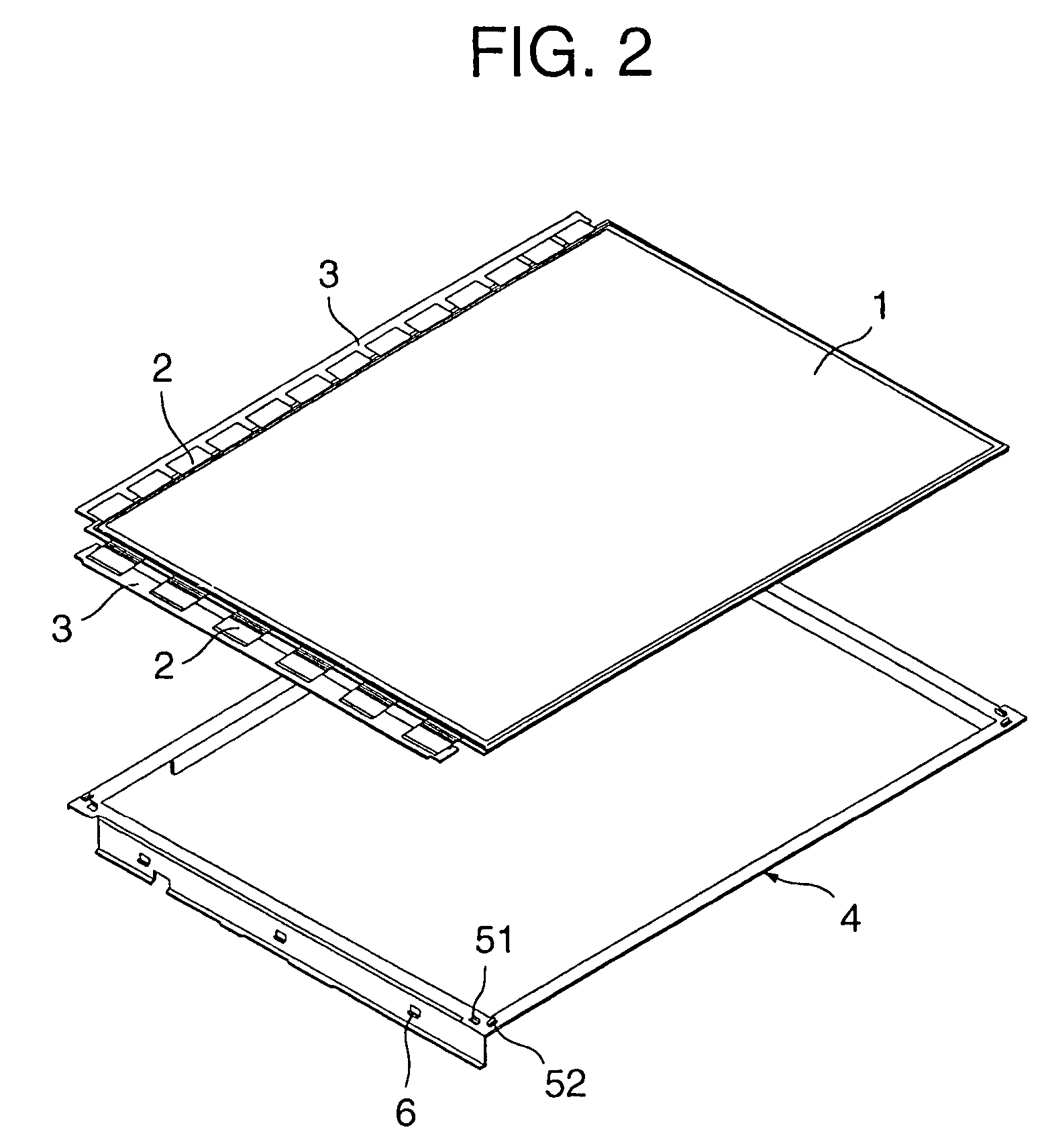
[0051]As shown in FIG. 2, one end of each of a plurality (13) of TCP's 2 is connected to an upper side of a liquid crystal panel 1 and one end of each of a plurality (6) of TCP's 2 is connected to a left side of a liquid crystal panel 1. The other ends of the TCP's 2 having the one ends connected to the upper side of the liquid crystal panel 1 are commonly connected to a circuit substrate 3 and the other ends of the TCP's 2 having the one ends connected to the left side of the liquid crystal panel 1 are commonly connected to another circuit substrate 3. The liquid crystal panel 1 is put on an area of an upper surface of a frame shaped chassis 4, which is defined by four pairs of protrusions 51 and 52 provided in four corners of the upper surface of the chassis 4. The liquid crystal pan...

third embodiment

[0079]the present invention will be described with reference to FIGS. 11 and 12.

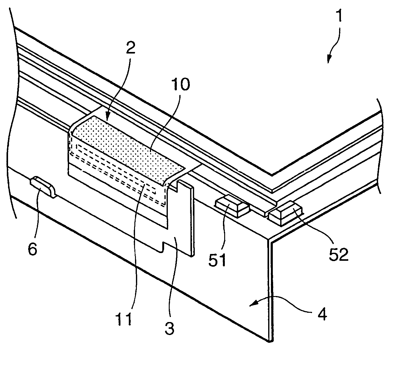
[0080]A wide single slit 10 formed in the TCP 2 will be described with reference to FIG. 11. A liquid crystal panel 1 is put on a region of an upper surface of a chassis 4, which is defined by four pairs of protrusions 51 and 52, and the wide slit 10 formed in a region of the TCP 2, where a circuit substrate 3 connected to the TCP is held by hook portions 6, is bent.

[0081]The wide slit 10 is similar to a combination of the main slit 7 and the sub slit 8 of the first embodiment shown in FIG. 4. That is, in the third embodiment, the wide slit 10 is formed over a region of the TCP 2, which corresponds to the region covering the main slit 7 and the sub slit 8 and the region between the slits 7 and 8 of the first embodiment, with an insulating film 23 thinner than the insulating film 23 of the first embodiment such that the portion of the wide slit 10 is easily bent as a whole. Therefore, a region 102 of the ...


PUM

PropertyMeasurementUnit
thicknessaaaaaaaaaa
thicknessaaaaaaaaaa
thicknessaaaaaaaaaa

Abstract

In a flat panel display device, in which a display panel 1 loosely fitted on a main surface of a chassis 4 and circuit substrates held in hook portions provided on side surfaces of the chassis are connected each other through TCP's by bending the latter TCP's, and a method for manufacturing the same device, a main slit for a rounded portion of each TCP is formed in a rounded portion of the TCP and an auxiliary sub slit is also formed adjacent to the main slit. In order to reduce the peeling force exerted on connecting / fixing portions between the TCP's and the display panel, the circuit substrate is pulled up by bending the main and sub slits and then returning the sub slit to a flat state to insert the circuit substrate into the hook portions.

Description

CROSS REFERENCE TO RELATED APPLICATION[0001]This application is a divisional of U.S. application Ser. No. 10 / 615,818, filed Jul. 9, 2003 now U.S. Pat. No. 6,819,371, which is in turn a divisional of U.S. application Ser. No. 09 / 613,476, filed Jul. 11, 2000, now U.S. Pat. No. 6,636,281, issued Oct. 21, 2003.BACKGROUND OF THE INVENTION[0002]1. Field of the Invention[0003]The present invention relates to a connecting construction of a flat panel display device such as a liquid crystal display device and a drive circuit substrate thereof and, particularly, to a flat panel display device having a construction, in which a display panel provided with a plurality of TCP's (Tape Carrier Packages) is easily detachably mounted on a casing of the flat panel display device, and a manufacturing method thereof.[0004]2. Description of the Prior Art[0005]As a flat panel display device, a liquid crystal display device, a plasma display device and an electroluminescence device, etc., are well known an...

Claims


Application Information

Patent Timeline
Patent Type & Authority Patents(United States)
IPC IPC(8): G02F1/1333G02F1/1345G02F1/13H05K1/00H05K1/14
CPCG02F1/13452H05K1/028H05K2201/10681H05K2201/0133H05K2201/0394H05K1/147G02F1/1345
Inventor KANATSU, TSUTOMU
Owner GOLD CHARM LTD
Why Eureka
Try Eureka