

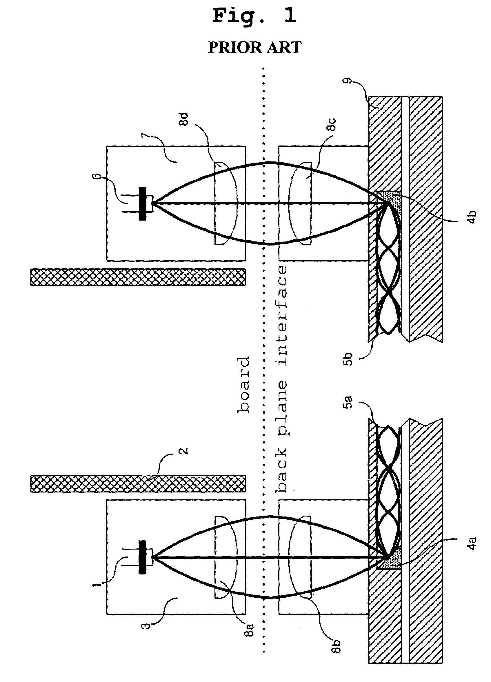
Printed circuit board with opto-via holes and process of forming the opto-via holes
a technology of printed circuit boards and opto-via holes, which is applied in the direction of printed circuit non-printed electric components association, electronic connection formation of printed elements, instruments, etc., can solve the problems of degrading the light transmissivity of the pcb, no commercial process by which the waveguide or glass plate is inserted into the pcb and connected to components outside the pcb, etc., and achieves the effect of stably transmitting a signal
- Summary
- Abstract
- Description
- Claims
- Application Information
AI Technical Summary
Benefits of technology
Problems solved by technology
Method used
Image

Examples
Embodiment Construction
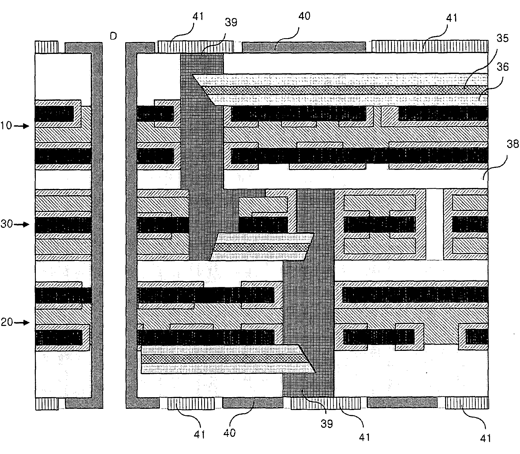
[0033]Reference numerals are made to the drawings, in which the same reference numerals are used throughout the different drawings to designate the same or similar components.
[0034]First Process: A Process of Forming Opto-via Holes in an Outer Layer
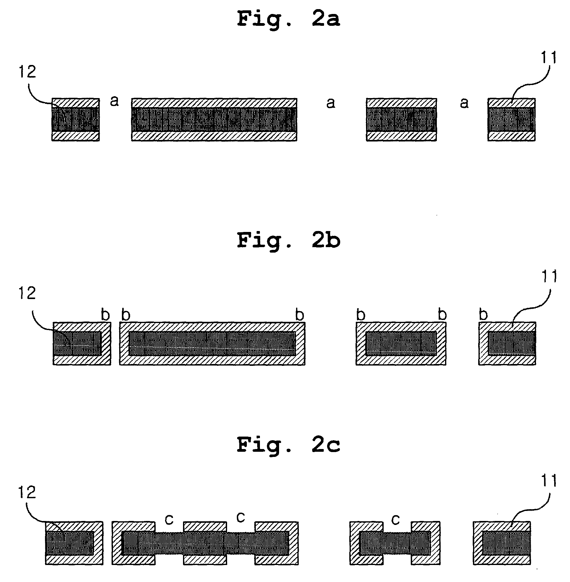
[0035]FIGS. 2a to 2f are sectional views stepwisely illustrating the formation process of the opto-via holes in the outer layer of a PCB according to an embodiment of the present invention.
[0036]In detail, FIG. 2a illustrates a forming step of a plurality of via holes on a copper clad laminate (CCL) using a drill, FIG. 2b illustrates a plating step of an inner wall of each via hole, and FIG. 2c illustrates a patterning step of a plated portion on the copper clad laminate by an exposing and an etching process. Additionally, FIG. 2d illustrates a layering step of the patterned copper clad laminates using an insulating resin adhesive, and in FIG. 2e, the adhesive on a position on which the opto-via holes are to be formed is removed, thereby ...
PUM
 Abstract
Description
Claims
Application Information