Method for the production of thin layer chip resistors

a technology of thin film and resistor, which is applied in the direction of resistors, cable/conductor manufacturing, decorative arts, etc., can solve the problems of higher manufacturing cost, more time-consuming successive processing of individual resistors and/or resistor lands, and disadvantages of resistor lands

Inactive Publication Date: 2006-02-14
BCCOMPONENTS HLDG
View PDF10 Cites 2 Cited by
  • Summary
  • Abstract
  • Description
  • Claims
  • Application Information

AI Technical Summary

Benefits of technology

[0007]It is an object of the present invention to provide a method for manufacturing thin-film chip resistors which provides a high precision of the resistors produced and at the same time simplifies and accelerates the production to reduce the manufacturing cost.
[0009]The invention allows to manufacture extremely cheap thin-film chip resistors benefiting from the advantages of a lithographic technology with the structuring being performed directly and, in contrast to photolithography, in a single process step. Compared with the aforementioned U.S. Pat. No. 5,978,392, the invention allows a faster and hence cheaper manufacturing of chip components because the structure is not “written” by a focussed laser beam but formed by a direct exposure of a whole or even several whole components using one or several laser shots.

Problems solved by technology

Components manufactured in this way normally are of a higher quality with the drawback of higher manufacturing cost.
The elimination of photolithography and the utilisation of thick-film contacts may help to reduce the cost, but implies the disadvantage of more time-consuming successive processing of the individual resistors and / or resistor lands.

Method used


Image

  • Method for the production of thin layer chip resistors
  • Method for the production of thin layer chip resistors
  • Method for the production of thin layer chip resistors

Examples


Embodiment Construction

[0007]It is an object of the present invention to provide a method for manufacturing thin-film chip resistors which provides a high precision of the resistors produced and at the same time simplifies and accelerates the production to reduce the manufacturing cost.

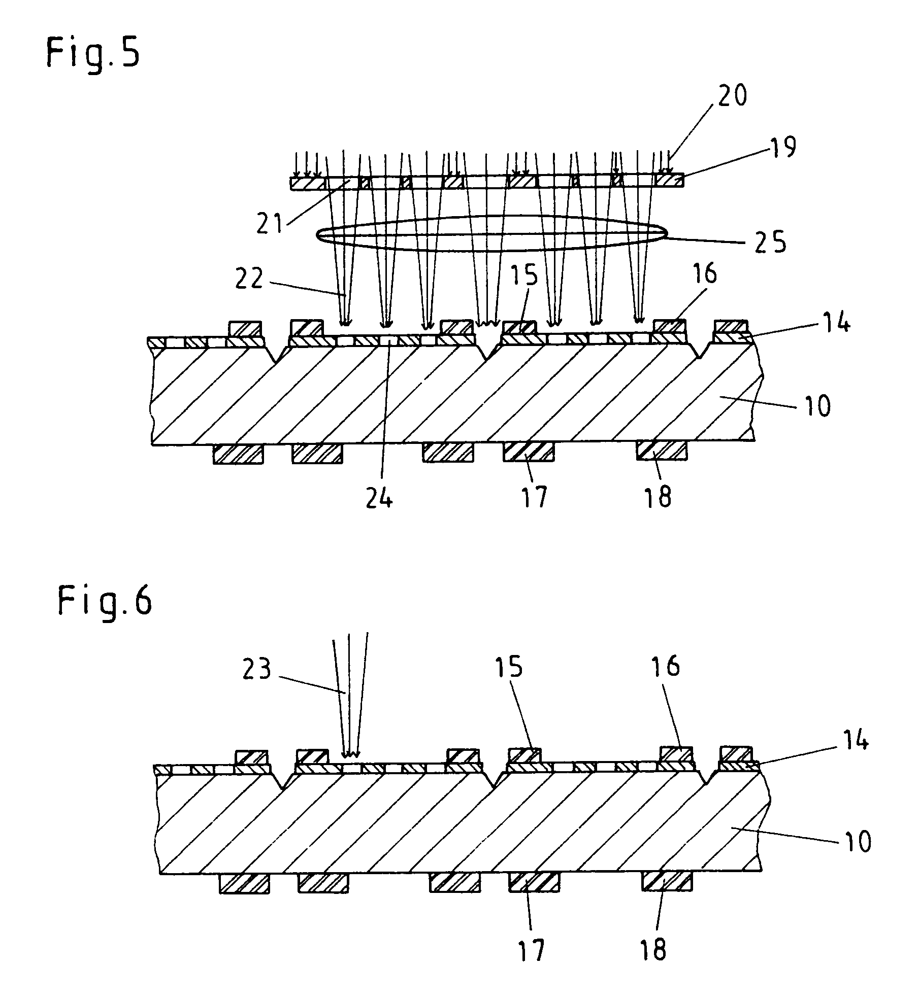
[0008]This object is achieved by the entirety of characteristics set forth in claim 1. The crux of the invention is to use a laser-lithographic direct exposure process wherein one or several complete resistors are structured by a single exposure (a “laser shot”) through an appropriately structured mask covering the entire region of resistors in order to form the lands of the individual resistors.

[0009]The invention allows to manufacture extremely cheap thin-film chip resistors benefiting from the advantages of a lithographic technology with the structuring being performed directly and, in contrast to photolithography, in a single process step. Compared with the aforementioned U.S. Pat. No. 5,978,392, the invention allows a ...


PUM

PropertyMeasurementUnit
wavelengthsaaaaaaaaaa
lengthaaaaaaaaaa
widthaaaaaaaaaa

Abstract

A method for manufacturing thin-film chip resistors, in which method a resistor layer (14) and a contact layer (15, 16) are applied onto the upper surface of a substrate (10) and structured using laser light so as to form on said substrate (10) a plurality of adjacent, separate resistor lands (24) having a predetermined approximate resistance value, allows the simplified and cheap manufacturing by performing the electrical insulation of the resistor elements (24) and the structuring of the individual resistor lands (24) for the entire resistor land simultaneously by means of a laser-lithographic direct exposure method.

Description

TECHNICAL FIELD[0001]The present invention relates to the field of manufacturing passive electronic components. It is directed to a method for manufacturing thin-film chip resistors according to the specification set forth in claim 1.[0002]Such a method is known, for example, from U.S. Pat. No. 5,978,392.PRIOR ART[0003]Methods for manufacturing thick-film resistors wherein the resistor and contact layers are applied as paste patterns by screen printing are generally known. In this manner, it is possible to manufacture very cheap components.[0004]Methods for manufacturing thin-film resistors or thin-film chip resistors are also known wherein the resistor and contact layers are applied by sputtering / vacuum evaporation and subsequently are structured in a photolithographic process step. Components manufactured in this way normally are of a higher quality with the drawback of higher manufacturing cost.[0005]The aforementioned U.S. Pat. No. 5,976,392 describes the manufacturing of a thin...

Claims


Application Information

Patent Timeline
Patent Type & Authority Patents(United States)
IPC IPC(8): H01L21/02H01C17/06H01C17/00H01C17/242
CPCH01C17/003H01C17/006H01C17/242Y10S438/94Y10S430/146
Inventor WERNER, WOLFGANGWOLF, HORSTKUEHL, REINER WILHELM
Owner BCCOMPONENTS HLDG
Why Eureka
Try Eureka