Testing memory access signal connections

a technology of memory access and signal connection, which is applied in the direction of electronic circuit testing, hardware monitoring, instruments, etc., can solve the problems of increasing the difficulty of gaining access to deeply embedded portions of the integrated circuit with no direct connection to the external pins of the integrated circuit, increasing the difficulty of designing appropriate test patterns to provide comprehensive test coverage, and increasing the need for testing in this way

Active Publication Date: 2006-02-14
ARM LTD
View PDF27 Cites 1 Cited by
  • Summary
  • Abstract
  • Description
  • Claims
  • Application Information

AI Technical Summary

Benefits of technology

[0013]The invention recognizes and exploits the feature that whilst memory size will vary (or a memory may not be present at all) and accordingly make some memory access signal connections optional or changed between different memory size implementations, a large number of these memory access signal connections will remain unchanged. Thus, the system may be arranged to use scan chain cells on those memory access signal connections which are variable between different implementations to allow these to be separately tested by their own test pattern whereas the memory access signal connections which are common between different implementations may be tested by being exercised by the data processing circuit concerned and the responses therefrom observed. In this way, there is a reduced requirement for scan chain cells in the integrated circuit as a whole and on the potentially timing limiting critical paths of the memory access signal connections. Furthermore, the number of different test patterns which need to be provided is reduced to a more acceptable level.
[0014]In preferred embodiments of the invention, the subset of memory access signal connections which are provided with scan chain cells are ones from which diagnostic signal data is captured but does not need to be applied by scan chain cell mechanisms. Scan chain cells which only capture data need not utilize a multiplexer in the critical data path so reducing the timing constraints which can be introduced by scan chain cell insertion. Memory access signal connections of the type from which data is normally only required to be captured include memory address signal connections.

Problems solved by technology

As integrated circuits increase in complexity and have an increasing number of functional units embedded therein, the need for test in this way increases and the difficulty of gaining access to deeply embedded portions of the integrated circuit with no direct connection to the external pins of the integrated circuit also increases.
These problems are further compounded in that different functional elements within the integrated circuit may be designed and produced by different suppliers who may not release full details of the design of their functional unit as this is proprietary information.
This makes the design of appropriate test patterns to provide comprehensive test coverage more difficult.
Whilst this approach works well in many cases, a difficulty arises when the particular functional unit may be connected to a variety of different forms of additional circuitry which necessitate different test patterns to be used.
However, the memory access signal connections are often timing critical signal paths and the additional delay that may be introduced by inserting a multiplexer in these paths so as to accommodate a scan chain cell is a significant disadvantage.
However, such techniques are memory size specific and accordingly in order to deal with a variety of possible different memory sizes which may be attached, a disadvantageously large number of suitable test patterns need to be provided.

Method used


Image

  • Testing memory access signal connections
  • Testing memory access signal connections
  • Testing memory access signal connections

Examples


Embodiment Construction

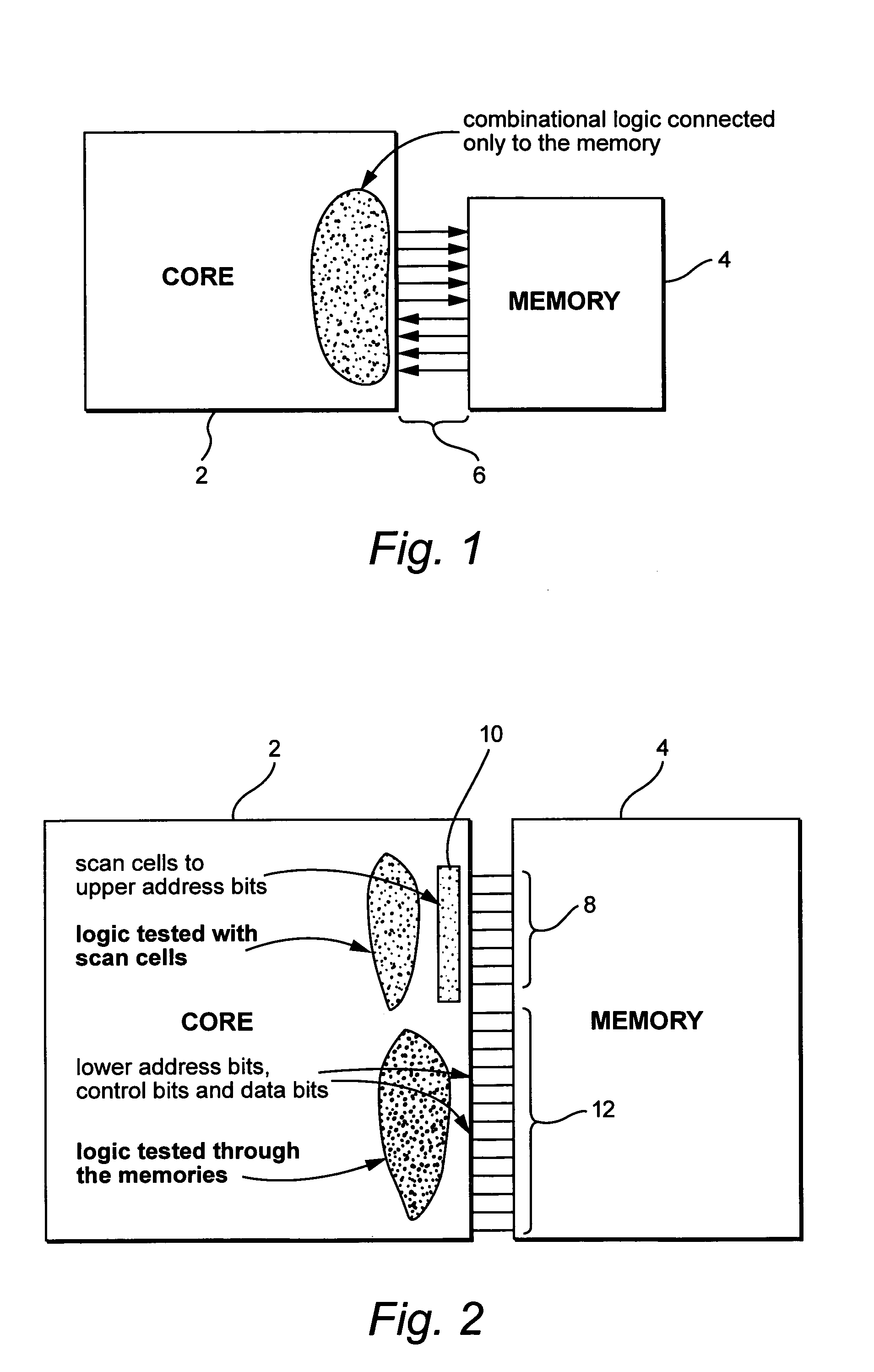
[0032]FIG. 1 shows a portion of an integrated circuit including a processor core 2 and a memory 4. Combinatorial logic within the processor core 2 is connected to the memory access port 6 and does not connect to other portions of the system to enable it to be otherwise tested. The memory 4 can vary in size depending upon the particular requirements of the system concerned (in some systems no memory may be present) and such variation in size can have an impact upon the precise form of the memory access port 6 and the memory access signal connections utilized. Accordingly, running a test operation upon the processor core 2 to exercise the memory access port 6 does not enable different sizes of memory 4 to be tested and would require different test pattern sets to be generated to stimulate the processor core 2 appropriately so as to accommodate all the different memory sizes possible for the memory 4. Memory size signals, which are usually tied during instantiation of a particular inte...


PUM


Abstract

In order to test the memory access signal connections between a data processing circuit, such as a processor core 2, and a memory 4, a subset of memory access signal connections 8 are provided with associated scan chain cells 10 so that they may be directly tested. The remainder memory access signal connections 12 which are common to all the expected configurations of the memory 4 are tested by being driven by the processor core 2 itself with data being passed through the memory and captured back within the processor core 2 for checking.

Description

BACKGROUND OF THE INVENTION[0001]1. Field of the Invention[0002]This invention relates to data processing systems. More particularly, this invention relates to the testing of memory access signal connections between a data processing circuit and a memory coupled to that data processing circuit.[0003]2. Description of the Prior Art[0004]It is known to provide testing mechanisms for testing integrated circuits when they have been manufactured to ensure that they operate correctly. One known technique is to include serial scan chains into which test patterns, such as automatically generated test patterns (AGTPs), may be scanned in and result values scanned out to verify correct operation of the manufactured integrated circuits. As integrated circuits increase in complexity and have an increasing number of functional units embedded therein, the need for test in this way increases and the difficulty of gaining access to deeply embedded portions of the integrated circuit with no direct co...

Claims


Application Information

Patent Timeline
Patent Type & Authority Patents(United States)
IPC IPC(8): G06F19/00G06F11/267G06F11/30
CPCG01R31/31717G06F11/267G11C29/022G11C29/02G11C2029/3202
Inventor MCLAURIN, TERESA LOUISEFREDERICK, FRANK DAVID
Owner ARM LTD
Why Eureka
Try Eureka