Capacitance probe for thin dielectric film characterization

a thin dielectric film and capacitance probe technology, applied in the direction of individual semiconductor device testing, semiconductor/solid-state device testing/measurement, instruments, etc., can solve the problems of high complexity of semiconductor manufacturing process, high difficulty in monitoring and measuring this dimension, and high difficulty in existing techniques for integrating circuits into semiconductor materials

Active Publication Date: 2006-02-21
VEECO METROLOGY
View PDF18 Cites 145 Cited by
  • Summary
  • Abstract
  • Description
  • Claims
  • Application Information

AI Technical Summary

Benefits of technology

[0017]The above summary of the present invention is not intended to describe each illustrated embodiment or every implementati

Problems solved by technology

The industry of semiconductor manufacturing involves highly complex techniques for integrating circuits into semiconductor materials.
Due to the large scale of circuit integration and the decreasing size of semiconductor devices, the semiconductor manufacturing process is prone to processing defects.
As semiconductor device film layer thickness approaches a few atomic levels, existing techniques for monitoring and measuring this dimension become very challenging due to measurement sensitivity scale.
For example, mea

Method used


Image

  • Capacitance probe for thin dielectric film characterization
  • Capacitance probe for thin dielectric film characterization
  • Capacitance probe for thin dielectric film characterization

Examples


Embodiment Construction

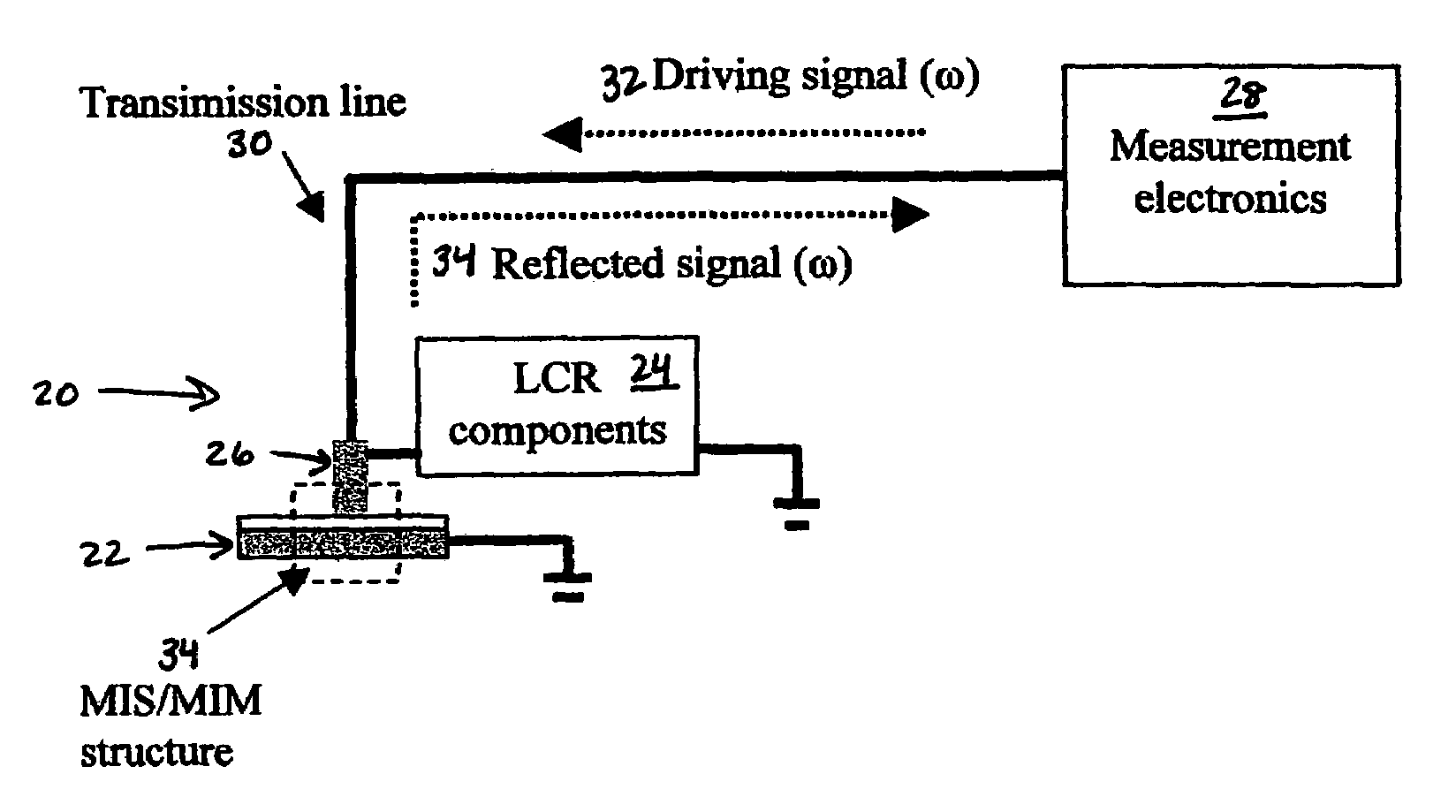
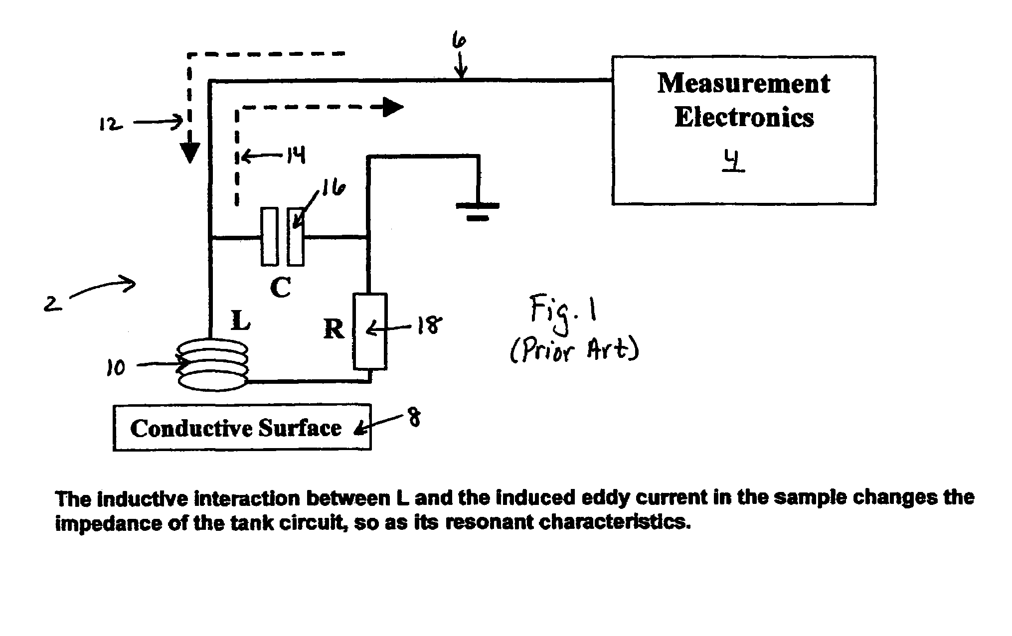
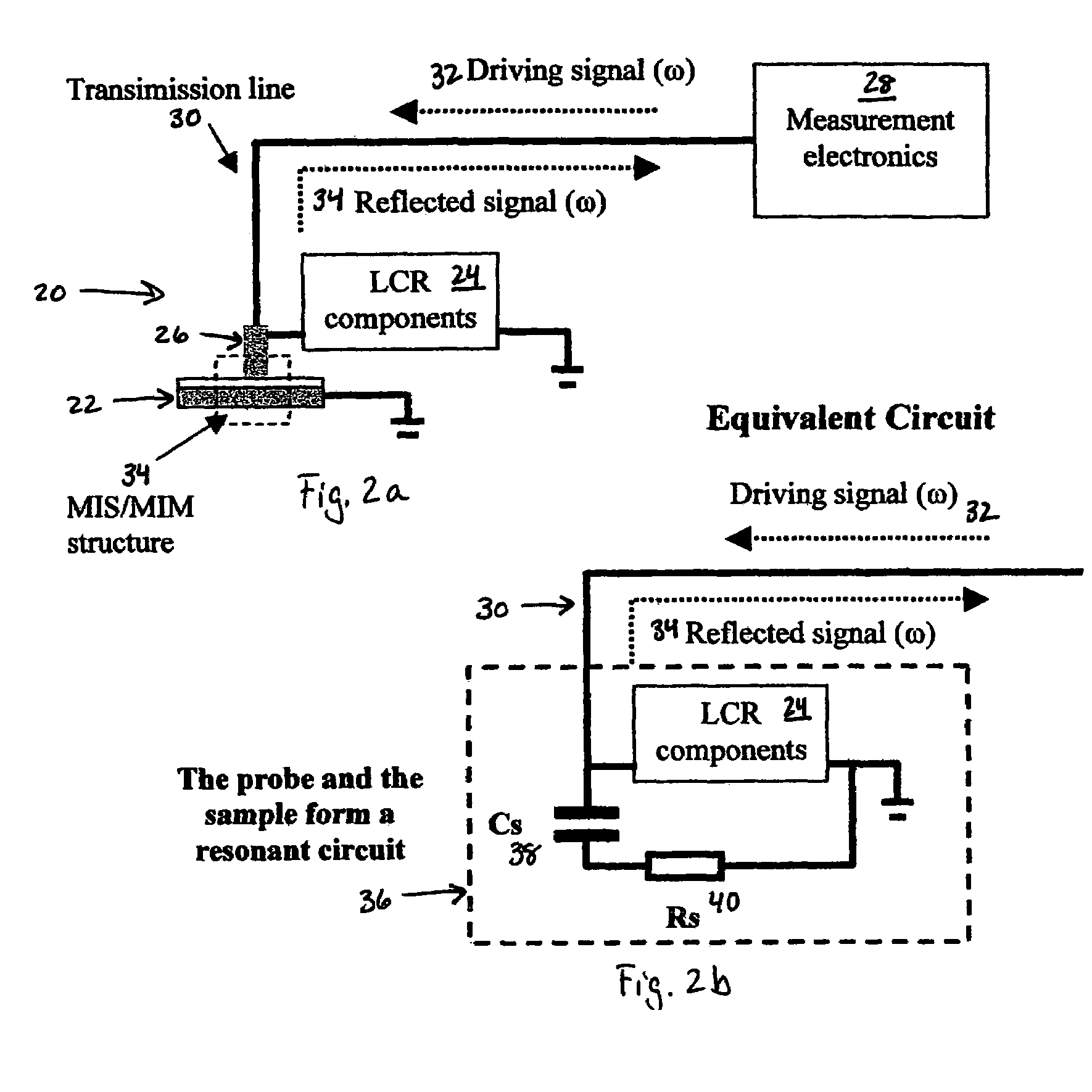
[0035]The capacitance probe for thin dielectric film characterization of the present invention provides a highly sensitive capacitance measurement method and reduces the contact area needed to obtain such a measurement. A preferred embodiment of the capacitance probe of the present invention is connected to a measurement system by a transmission line and comprises a center conductive tip and LCR components between the center conductor and the ground of the transmission line. When the probe tip is in contact with a sample, an MIS or MIM structure is formed, with the LCR components and the capacitance of the MIS or MIM structure forming a resonant circuit. By sending a high frequency driving signal to the probe and by measuring the reflected signal from the probe through the transmission line, the resonant characteristic of the resonant circuit can be obtained because the reflected signal has minimum power at the resonant frequency of the probe circuit. The capacitance of the MIS or M...


PUM


Abstract

A capacitance probe for thin dielectric film characterization provides a highly sensitive capacitance measurement method and reduces the contact area needed to obtain such a measurement. Preferably, the capacitance probe is connected to a measurement system by a transmission line and comprises a center conductive tip and RLC components between the center conductor and the ground of the transmission line. When the probe tip is in contact with a sample, an MIS or MIM structure is formed, with the RLC components and the capacitance of the MIS or MIM structure forming a resonant circuit. By sending a driving signal to the probe and measuring the reflected signal from the probe through the transmission line, the resonant characteristic of the resonant circuit can be obtained. The capacitance of the MIS or MIM structure is obtainable from the resonant characteristics and the dielectric film thickness or other dielectric properties are also extractable.

Description

FIELD OF THE INVENTION[0001]The present invention generally relates to the field of film characterization in semiconductor devices. In particular, the present invention relates to a capacitance probe for use with a scanning probe microscope in determining a dielectric film thickness in semiconductor devices.BACKGROUND OF THE INVENTION[0002]The industry of semiconductor manufacturing involves highly complex techniques for integrating circuits into semiconductor materials. Multiple fine layers of metals and materials form these integrated circuits. To increase the speed and performance of devices utilizing integrated circuits, the size of semiconductor devices must be decreased. Due to the large scale of circuit integration and the decreasing size of semiconductor devices, the semiconductor manufacturing process is prone to processing defects. When the dimensions of semiconductor devices are decreased, the thickness of the various layers of metals and materials must be controlled more...

Claims


Application Information

Patent Timeline
IPC IPC(8): H01L21/66
CPCG01R27/2658
Inventor CHEN, DONG
Owner VEECO METROLOGY
Why Eureka
Try Eureka