Method of setting back bias of MOS circuit, and MOS integrated circuit

a technology of mos circuit and integrated circuit, which is applied in the direction of pulse generator, pulse technique, instruments, etc., can solve problems such as problems and effects to be solved

Inactive Publication Date: 2006-02-21
RENESAS ELECTRONICS CORP
View PDF26 Cites 66 Cited by
  • Summary
  • Abstract
  • Description
  • Claims
  • Application Information

AI Technical Summary

Problems solved by technology

However, problems and effects to be solved by the ap...

Method used


Image

  • Method of setting back bias of MOS circuit, and MOS integrated circuit
  • Method of setting back bias of MOS circuit, and MOS integrated circuit
  • Method of setting back bias of MOS circuit, and MOS integrated circuit

Examples


first embodiment

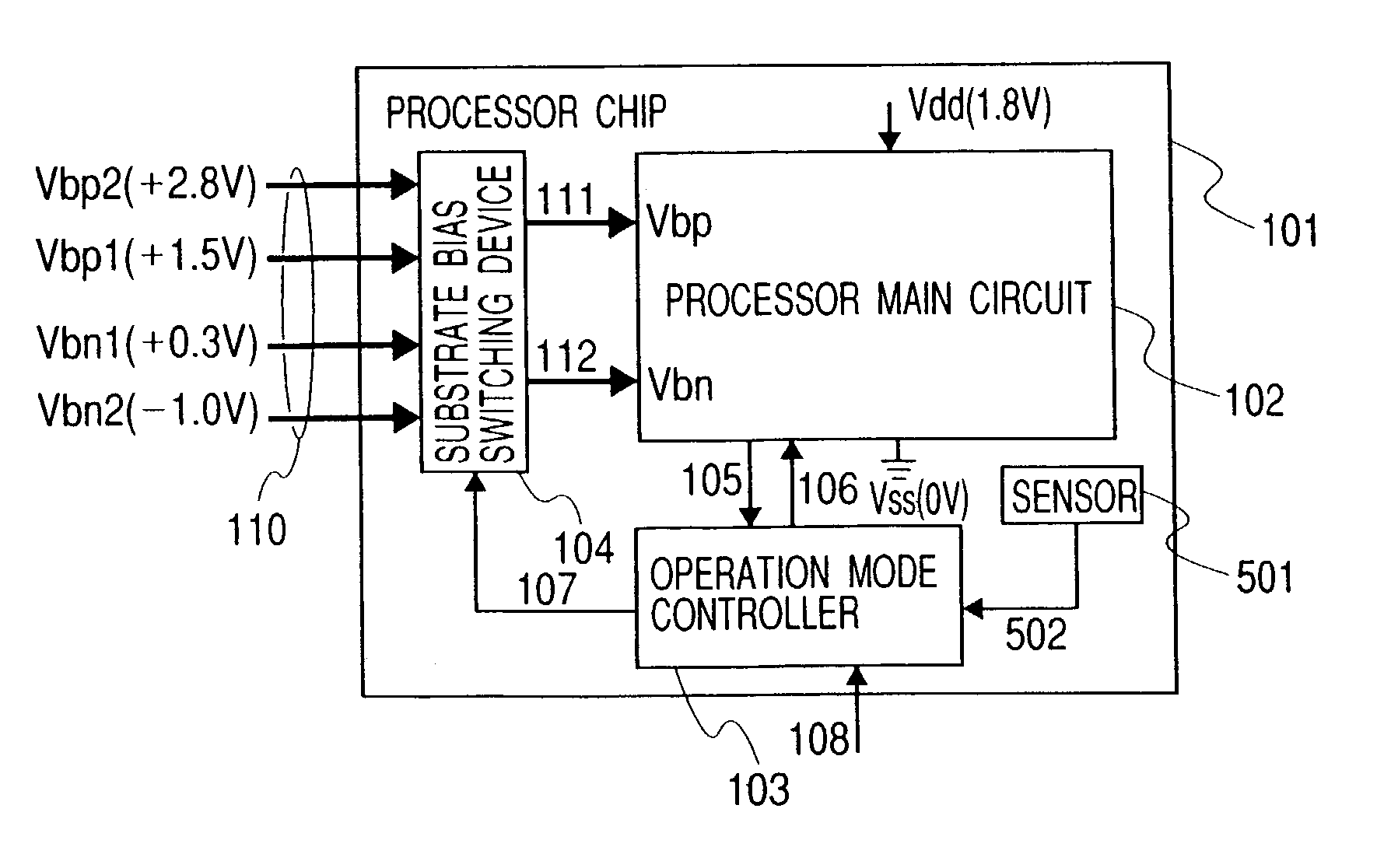
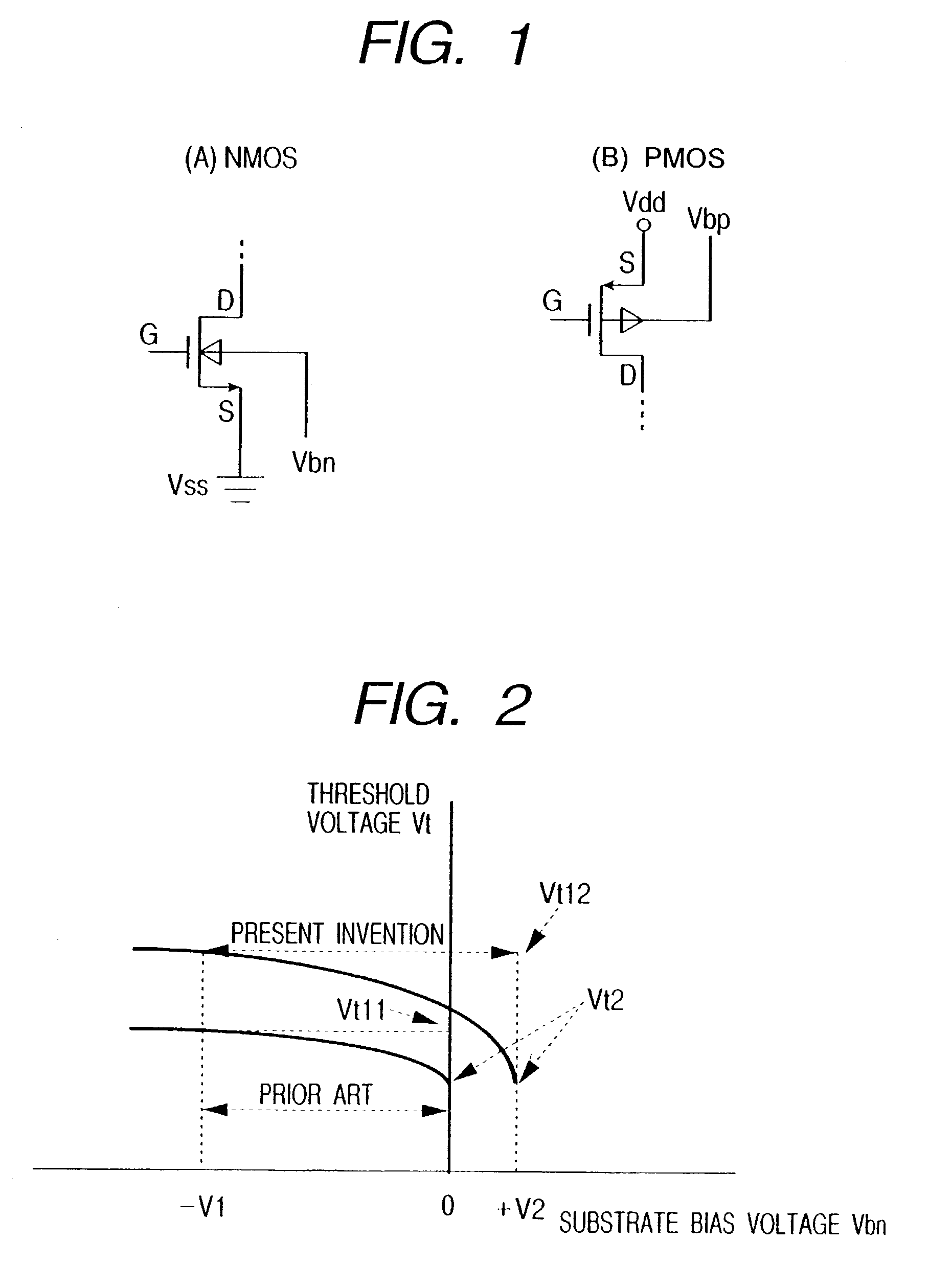
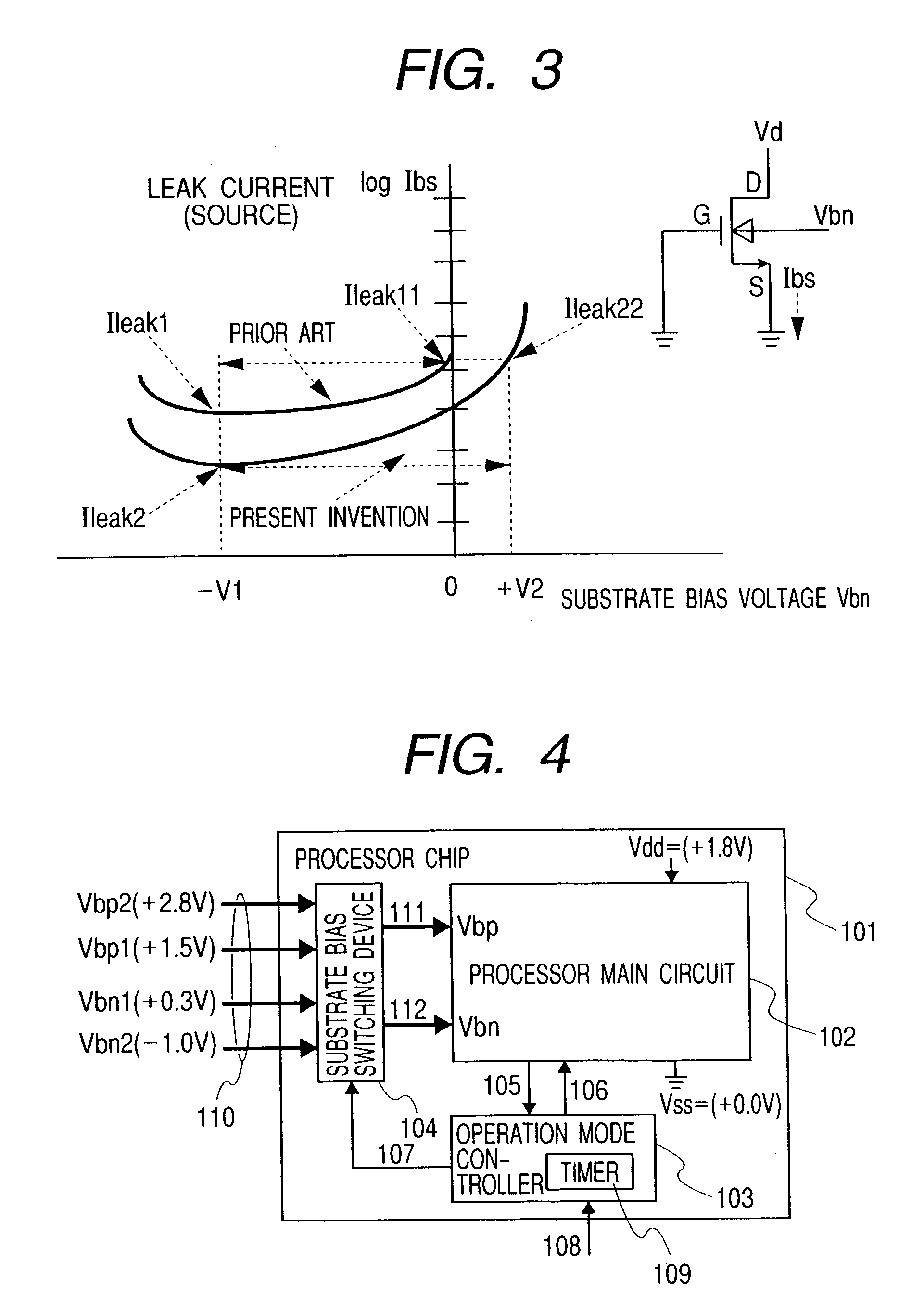
[0086]A block diagram showing a processor chip to which the present invention is applied, is shown in FIG. 4. In FIG. 4, a processor chip 101 is an LSI chip having a circuit of a CMOS structure, which includes a processor main circuit 102, an operation mode controller 103, and a substrate bias switching device 104. The substrate bias switching device 104 receives therein a bias voltage 110 comprised of substrate bias voltages Vbp1 and Vbp2 for a p channel type MOSFET, and substrate bias voltages Vbn1 and Vbn2 for an n channel type MOSFET, outputs a bias voltage 111 for the p channel type MOSFET and a bias voltage 112 for the n channel type MOSFET, and transmits them to a bias voltage Vbp for a p channel type MOSFET of the processor main circuit 102 and a bias voltage Vbn for an n channel MOSFET thereof.

[0087]When the processor main circuit 102 is in a normal mode, the substrate bias switching device 104 sets the bias voltage Vbp for the p channel type MOSFET to Vbp1 and sets the bia...

second embodiment

[0094]In the present embodiment, the processor main circuit 102 is formed within the p well 302 different from the operation mode controller 103 and the substrate bias switching device 104. Thus, the influence of substrate bias control is effected on the processor main circuit 102 alone, and hence the operation mode controller 103 and substrate bias switching device 104 can avoid its influence. Schematic cross-sectional views of device structures each showing a semiconductor integrated circuit device like the processor chip 101, to which the present invention is applied, are respectively shown in FIGS. 7 and 8. In the present embodiment, an SOI structure is used. Namely, an insulating layer (oxide) is formed in the surface of a semiconductor substrate, and a p type well region and an n type well region are formed in the surface of the insulating layer, thereby forming an n channel type MOSFET and a p channel type MOSFET in a manner similar to the above. Back bias voltage terminals V...

third embodiment

[0105]A block diagram of a processor chip according to the present invention is shown in FIG. 11. The triple well structure shown in FIG. 6 or the SOI structures shown in FIGS. 7 and 8 is considered as a basic device structure of a processor chip 601. In the processor chip 601 shown in FIG. 11, a processor main circuit comprises a plurality of function modules like a CPU 604, a module A606 and a module B608. The respective function modules exist on different well regions so as to be separated from one another and is placed under the uninfluence of substrate bias control of other function modules.

[0106]Each of the function modules includes ones given in smaller units such as a CPU, an FPU, a cache, or a computing unit, etc. Substrate bias switching devices 605, 607 and 609 are respectively provided in association with the respective function modules 604, 606 and 608 and respectively perform switching between substrate biases for the corresponding function modules in a manner similar ...


PUM


Abstract

In a MOS circuit comprising a plurality of MOSFETs constituting a digital circuit, an input signal is supplied to the digital circuit, and a first back bias voltage is supplied to a semiconductor substrate or a semiconductor well region in which the MOSFETs are formed, so that a pn junction between the semiconductor substrate or the semiconductor well region and a source region is brought to a forward voltage. In a non-operating state in which a circuit operation is suspended by the input signal supplied to the digital circuit as a fixed level, a second back bias voltage is applied to the semiconductor substrate or the semiconductor well region so that the pn junction between the semiconductor substrate or the semiconductor well region and the source region is brought to a reverse voltage.

Description

CROSS-REFERENCE TO RELATED APPLICATIONS[0001]This application is a continuation of application Ser. No. 09 / 890,170 filed Jul. 26, 2001, which is a 371 of International Application No. PCT / JP99 / 07034 filed Dec. 15, 1999.TECHNICAL FIELD[0002]The present invention relates to a method of setting back biases of a MOS circuit and a MOS integrated circuit, and principally to a technology effective for application to a technology for reducing a subthreshold leak current produced in a CMOS (Complementary MOS) circuit.BACKGROUND ART[0003]After the present invention has been brought to completion, the present inventors have investigated the known references about the following viewpoints A and B on the basis of the result of the invention. The viewpoint A is one wherein a potential at a semiconductor well in which an n channel type MOSFET or a p channel type MOSFET is formed, is biased in a weak forward direction with respect to a source potential. The viewpoint B is one wherein a potential at...

Claims


Application Information

Patent Timeline
IPC IPC(8): H03K3/01H01L21/761H01L27/092H01L27/12H03K3/356
CPCH01L21/761H01L27/1203H01L27/0928H03K3/356113
Inventor KUBO, MASAHARUHIRAKI, MITSURUMIZUNO, HIROYUKIIKEDA, SYUJI
Owner RENESAS ELECTRONICS CORP
Why Eureka
Try Eureka