Base material cutting method, base material cutting apparatus, ingot cutting method, ingot cutting apparatus and wafer producing method

a cutting method and cutting method technology, applied in the field of base material cutting method, ingot cutting method, ingot cutting apparatus and wafer producing method, can solve the problems of large amount of ingot waste, insufficient small waste of ingot, and needing a thick cutting margin

Inactive Publication Date: 2006-02-28
CANON KK
View PDF4 Cites 2 Cited by
  • Summary
  • Abstract
  • Description
  • Claims
  • Application Information

AI Technical Summary

Benefits of technology

[0017]Here in order to improve the processing efficiency, a plurality of optical wave guides may be aligned in parallel in the axial direction of the crystalline ingot or other base material to guide light simultaneously to a plurality of parts of the base material and thereby process these plurality of parts simultaneously. Also in this case, light from a single light source may be made to enter the plurality of optical wave guides to minimize the necessary number of light sources.
[0021]This invention also provides an ingot cutting method or ingot cutting apparatus, wherein a crystalline ingot is positioned within an etching gas and the etching gas is excited by illumination of light from a light source onto the crystalline ingot via a sheet-like or bar-like optical wave guide, thereby making a component of the etching gas react chemically with a component of the crystalline ingot and volatilizing the component of the crystalline ingot to cut the crystalline ingot and obtain wafers, and wherein the crystalline ingot is positioned in an inclined manner with respect to the horizontal direction so that a wafer that has been cut will not tilt towards the optical wave guide nor towards the remaining crystalline ingot side and wafers are thereupon obtained one by one by sequentially cutting the crystalline ingot.

Problems solved by technology

However, with such machine cutting methods, a thick cutting margin is necessary and a large amount of the ingot is wasted.
The waste of ingot therefore cannot be made adequately small even when the cutting method proposed in the abovementioned publication is used.
However, if a light source is to be provided for each part that is cut, the arrangement of the cutting apparatus will become complicated and the cost may become high.
However, if a plurality of wafers or other thin plates are simply cut out simultaneously, these thin plates that have been cut out may collide with each other, thereby leading to flawing of the thin plates.
Though this problem can be resolved by securely supporting the plurality of thin plates that are cut out so that the thin plates will not tilt or become overlapped, this is difficult to achieve in actuality.

Method used


Image

  • Base material cutting method, base material cutting apparatus, ingot cutting method, ingot cutting apparatus and wafer producing method
  • Base material cutting method, base material cutting apparatus, ingot cutting method, ingot cutting apparatus and wafer producing method
  • Base material cutting method, base material cutting apparatus, ingot cutting method, ingot cutting apparatus and wafer producing method

Examples


Embodiment Construction

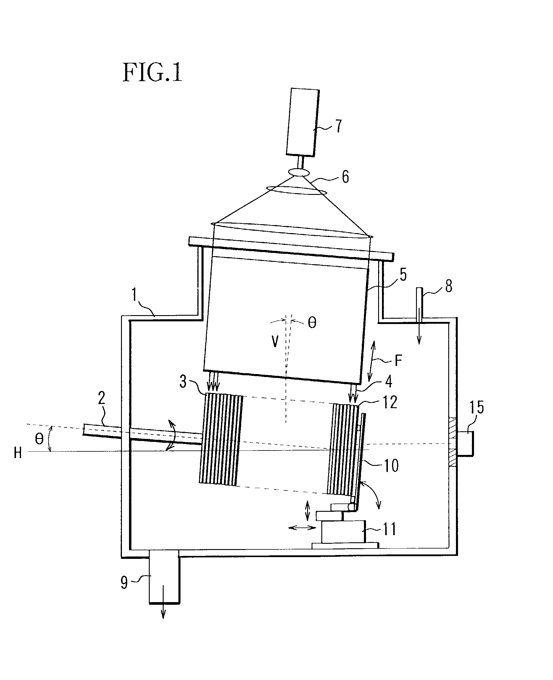
[0040]Hereinafter, preferred embodiments of the invention will be described in detail with reference to the drawings.

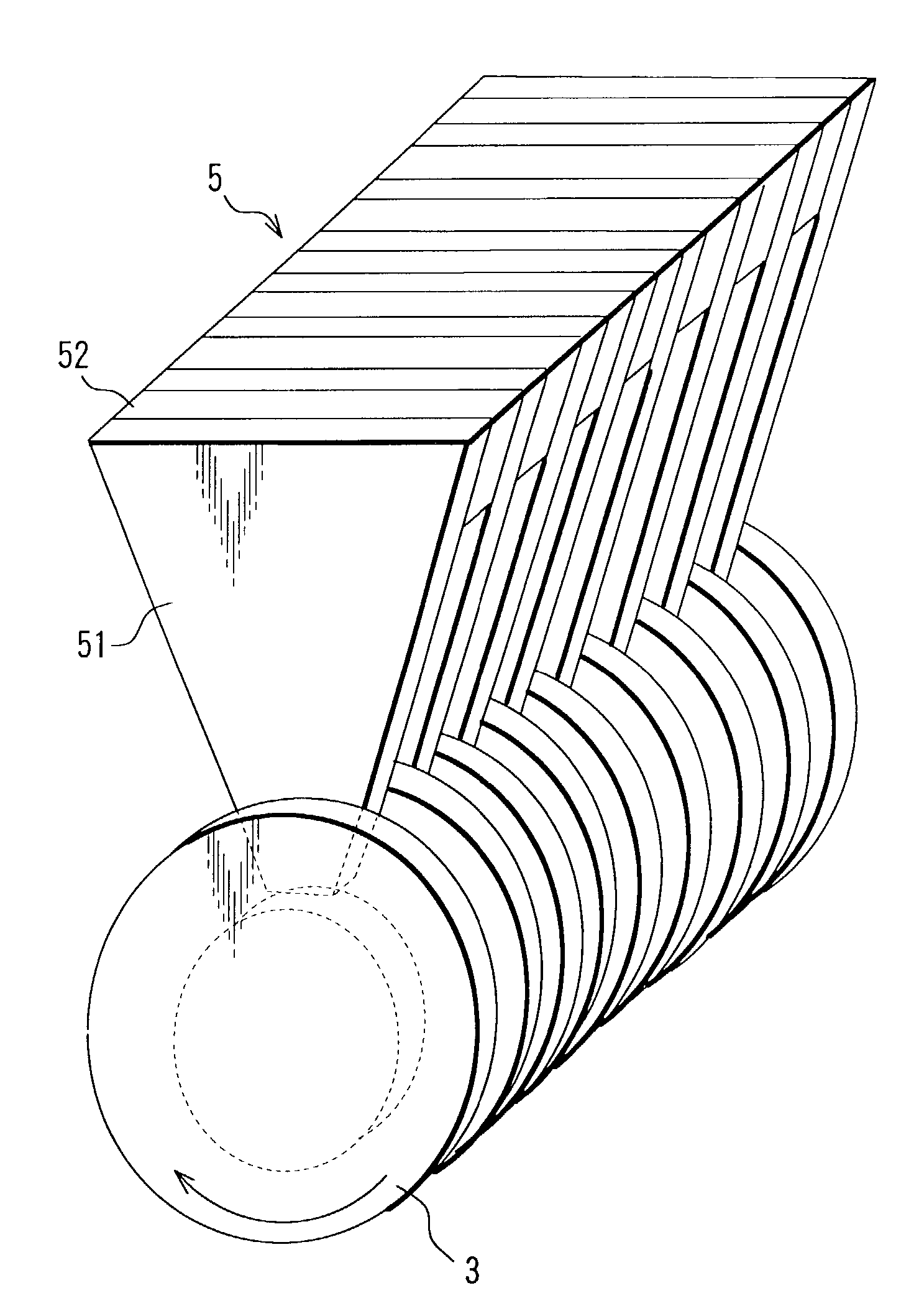
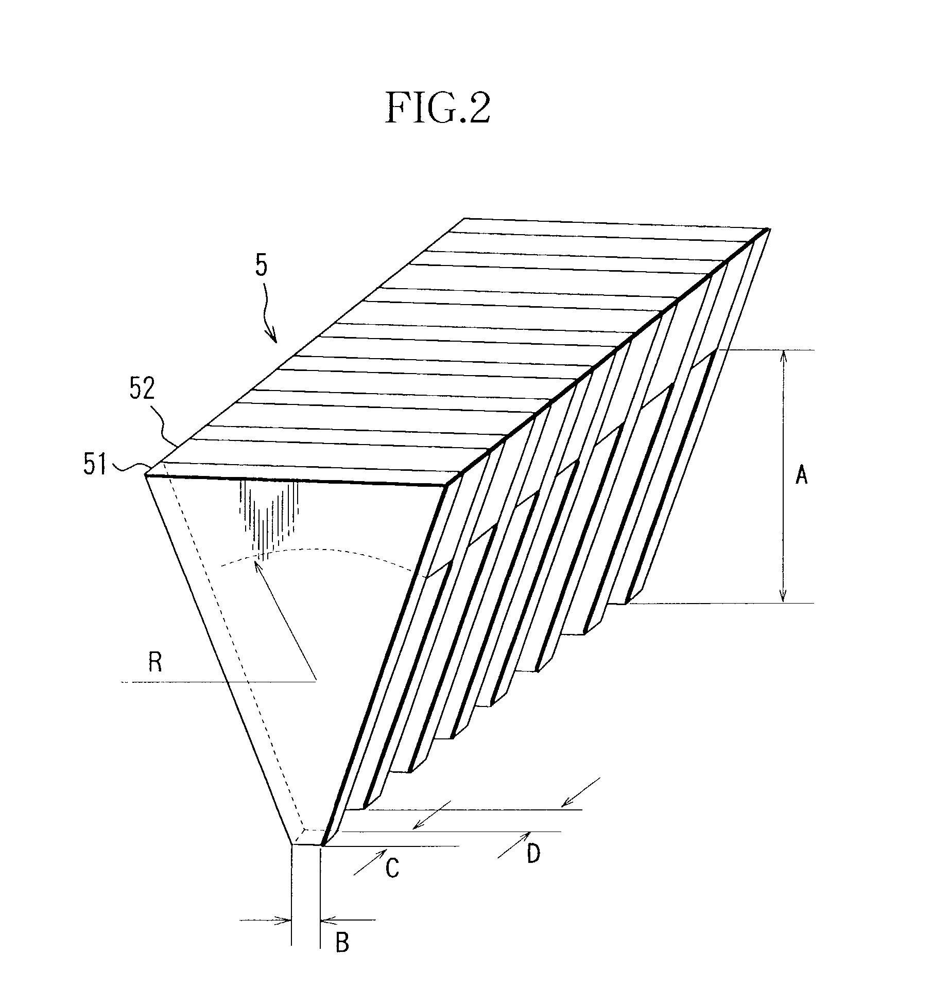
[0041]FIG. 1 shows the overall arrangement of an ingot cutting apparatus, which is an embodiment of this invention. In this FIG., 1 is a chamber and an etching gas supply piping 8, for supplying etching gas into the chamber 1, is connected to the upper part of the chamber 1. Also, an exhaust piping 9, for evacuating or drawing out etching gas from the interior of chamber 1, is connected to the lower part of the chamber 1. An unillustrated vacuum pump is connected to the exhaust piping 9.

[0042]As the etching gas, a gas comprising at least one component of NF3, CCl2F2, CF4, C2F6, C3F8, CHF3, CCl4, SF6, CCl3F, HCl and HF is used, and a solitary gas may be used or a mixed gas of two or more types of gases may be used.

[0043]Anti-corrosion treatment by at least one component of SiC, AlN, SiN, Al2O3, AlF3, FRP treatment material, and CRP treatment material is applied to part...


PUM

PropertyMeasurementUnit
groove widthaaaaaaaaaa
thicknessaaaaaaaaaa

Abstract

This invention discloses an ingot cutting apparatus, wherein a crystalline ingot is positioned within an etching gas and a component of the etching gas is excited by illumination of light from a light source onto the crystalline ingot, thereby making a component of the etching gas react chemically with the component of the crystalline ingot and volatilizing the component of the crystalline ingot to cut the crystalline ingot and obtain wafers and wherein light from a light source is guided to the crystalline ingot via a sheet-like, bar-like, or fiber-like optical wave guide.

Description

BACKGROUND OF THE INVENTION[0001]1. Field of the Invention[0002]This invention relates to a cutting method and cutting apparatus by which a columnar (cylindrical) or prismatic (e.g. square pillar) base material, such as crystalline ingot, etc., is cut to obtain thin plates, such as wafers, etc., and to be more specific, relates to a cutting method and cutting apparatus by which thin plates, such as wafers, etc., are obtained by a photochemical reaction, etc. that makes use of light energy.[0003]2. Description of the Related Art[0004]Examples of processes, wherein a base material is cut into thin plates, include processes, wherein wafers, to be used for the manufacture of semiconductor devices, are cut from a columnar or prismatic crystalline ingot, comprising a crystal of Si or GaAs, etc.[0005]Among such methods of cutting wafers from an ingot, there are methods of cutting an ingot physically by means of a diamond blade saw or wire saw, etc. However, with such machine cutting method...

Claims


Application Information

Patent Timeline
Patent Type & Authority Patents(United States)
IPC IPC(8): H01L21/00B28D5/00B28D5/04
CPCB28D5/04B28D5/00
Inventor KAWASE, NOBUOOHTA, MASAKATSUTANAKA, NOBUYOSHI
Owner CANON KK
Why Eureka
Try Eureka