Memory redundancy programming

a memory device and programming technology, applied in the field of memory device programming redundancy, can solve the problems of limited time that the redundancy programming may take place, the device is very dense, and the manufacturer is not capable of producing memory devices that are completely defect-free or failure-fr

Inactive Publication Date: 2006-02-28
MICRON TECH INC
View PDF5 Cites 14 Cited by
  • Summary
  • Abstract
  • Description
  • Claims
  • Application Information

AI Technical Summary

Problems solved by technology

These devices are very densely packed, i.e., there is little space between them.
Generally, manufacturers are not capable of producing memory devices that are completely defect free or failure free.
Among the problems associated with implementing such redundancy programming may include the fact that a laser implementation requires a line of sight to invoke the laser energy; thereby the time that the redundancy programming may take place is limited.
If a memory device is packaged then the laser implementation would not be possible.
Additionally, in the large current method, large amounts of currents are required to provide controlled blowing of fuses, which may cause inefficiencies during manufacturing.
The anti-fuse method may also result in various inefficiencies in the manufacturing or memory devices, including problems created by the current pulse, and inefficiencies in detecting the programming.

Method used


Image

  • Memory redundancy programming
  • Memory redundancy programming
  • Memory redundancy programming

Examples


Embodiment Construction

[0024]Illustrative embodiments of the invention are described below. In the interest of clarity, not all features of an actual implementation are described in this specification. It will of course be appreciated that in the development of any such actual embodiment, numerous implementation-specific decisions must be made to achieve the developers' specific goals, such as compliance with system-related and business-related constraints, which will vary from one implementation to another. Moreover, it will be appreciated that such a development effort might be complex and time-consuming, but would nevertheless be a routine undertaking for those of ordinary skill in the art having the benefit of this disclosure.

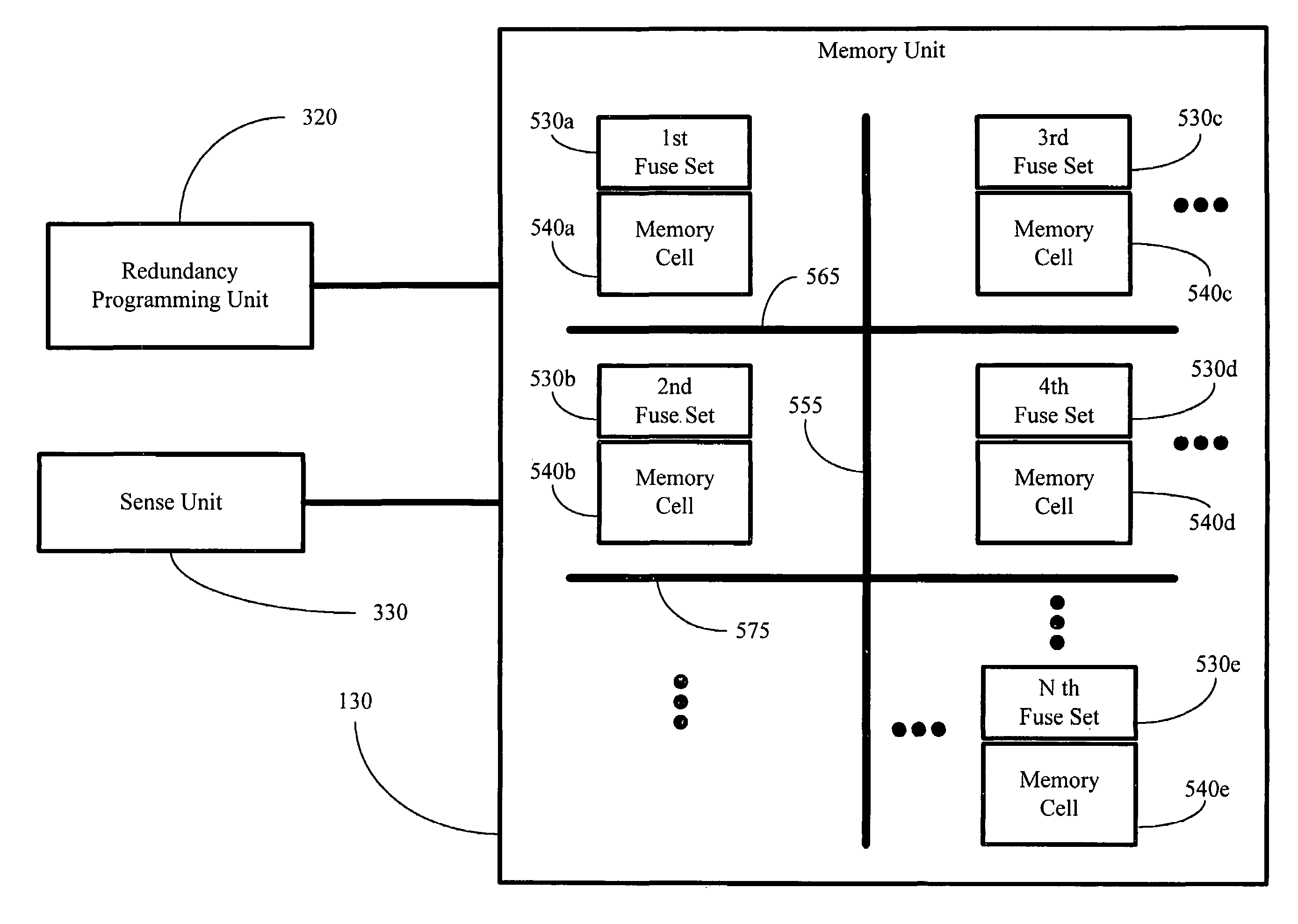
[0025]Embodiments of the present invention provide for implementing a redundancy programming utilizing an electron charge trapping technique to program a particular element of a memory device into an active state or to de-program a memory element into an inactive state. The prese...


PUM


Abstract

A method and apparatus is provided for performing a redundancy programming. The system of the present invention includes a device testing unit for performing a memory test. The system also includes a memory device operatively coupled to the device testing unit. The memory device includes an access transistor that includes a charge trapping area. A threshold voltage of the access transistor is modified upon trapping of charges in the charge trapping unit. The memory device also includes a memory element and a fuse associated with the memory element. The fuse is capable of entering an alternative state in response to modifying the threshold voltage of the access transistor. The state of the fuse may be used to program or de-program the memory element.

Description

BACKGROUND OF THE INVENTION[0001]1. Field of the Invention[0002]This invention relates generally to a semiconductor memory device, and, more specifically, to programming redundancy in memory devices.[0003]2. Description of the Related Art[0004]Modern integrated circuit devices are comprised of millions of semiconductor devices, e.g., transistors, formed above a semiconductor substrate, such as silicon. These devices are very densely packed, i.e., there is little space between them. Similarly densely packed electrically conducting lines may also be formed in the semiconductor substrate. By forming selected electrical connections between selected semiconductor devices and selected conducting lines, circuits capable of performing complex functions may be created. For example, bits of data may be stored by providing electrical current to a plurality of bit lines and an orthogonal plurality of word lines that may be electrically coupled to one or more capacitors in a semiconductor memory...

Claims


Application Information

Patent Timeline
Patent Type & Authority Patents(United States)
IPC IPC(8): G11C7/00G11C11/34G11C29/00
CPCG11C29/789G11C17/18
Inventor PAREKH, KUNAL R.
Owner MICRON TECH INC
Why Eureka
Try Eureka