Emissive display device and electroluminescence display device with uniform luminance

a technology of display device and light source, applied in the direction of static indicating device, discharge tube luminescnet screen, instruments, etc., can solve the problems of light emission and dim display area in such areas, and achieve the effect of efficient and reliabl

Inactive Publication Date: 2006-03-07
SANYO ELECTRIC CO LTD
View PDF9 Cites 27 Cited by
  • Summary
  • Abstract
  • Description
  • Claims
  • Application Information

AI Technical Summary

Benefits of technology

[0036]These arrangements allow efficient and reliable for...

Problems solved by technology

This light radiates outward through the transparent anode via the transparent insulator substrate, resulting in light emission.
The organic EL elements 160 located in display...

Method used


Image

  • Emissive display device and electroluminescence display device with uniform luminance
  • Emissive display device and electroluminescence display device with uniform luminance
  • Emissive display device and electroluminescence display device with uniform luminance

Examples


Embodiment Construction

[0045]The display device of the present invention will now be described.

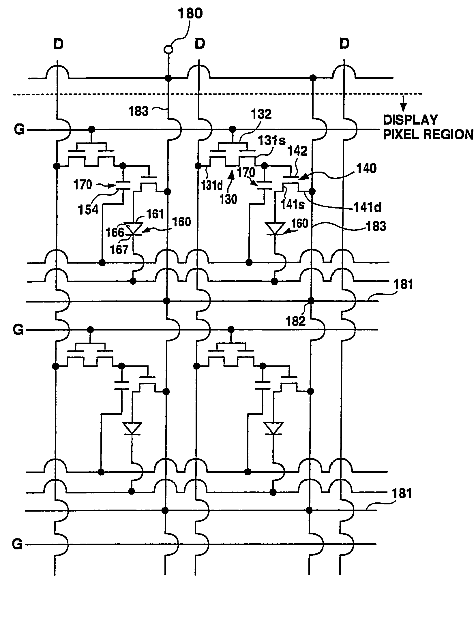
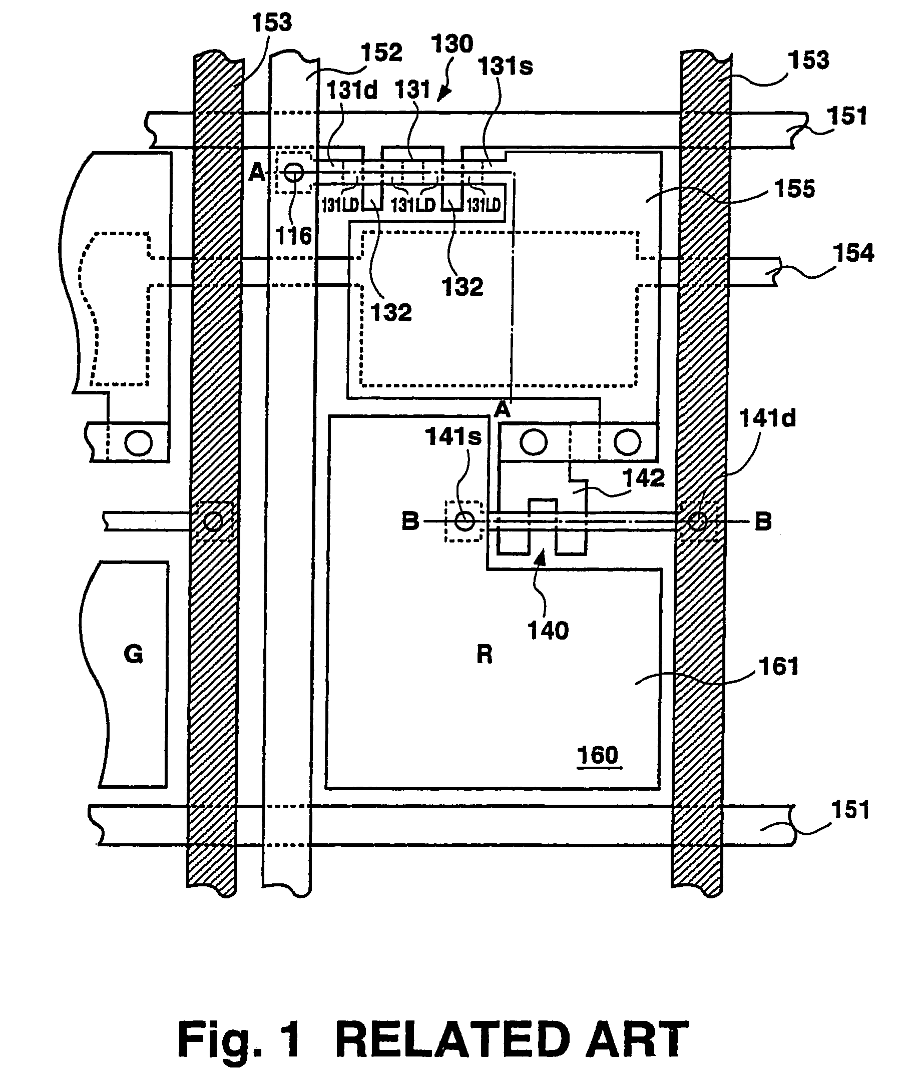
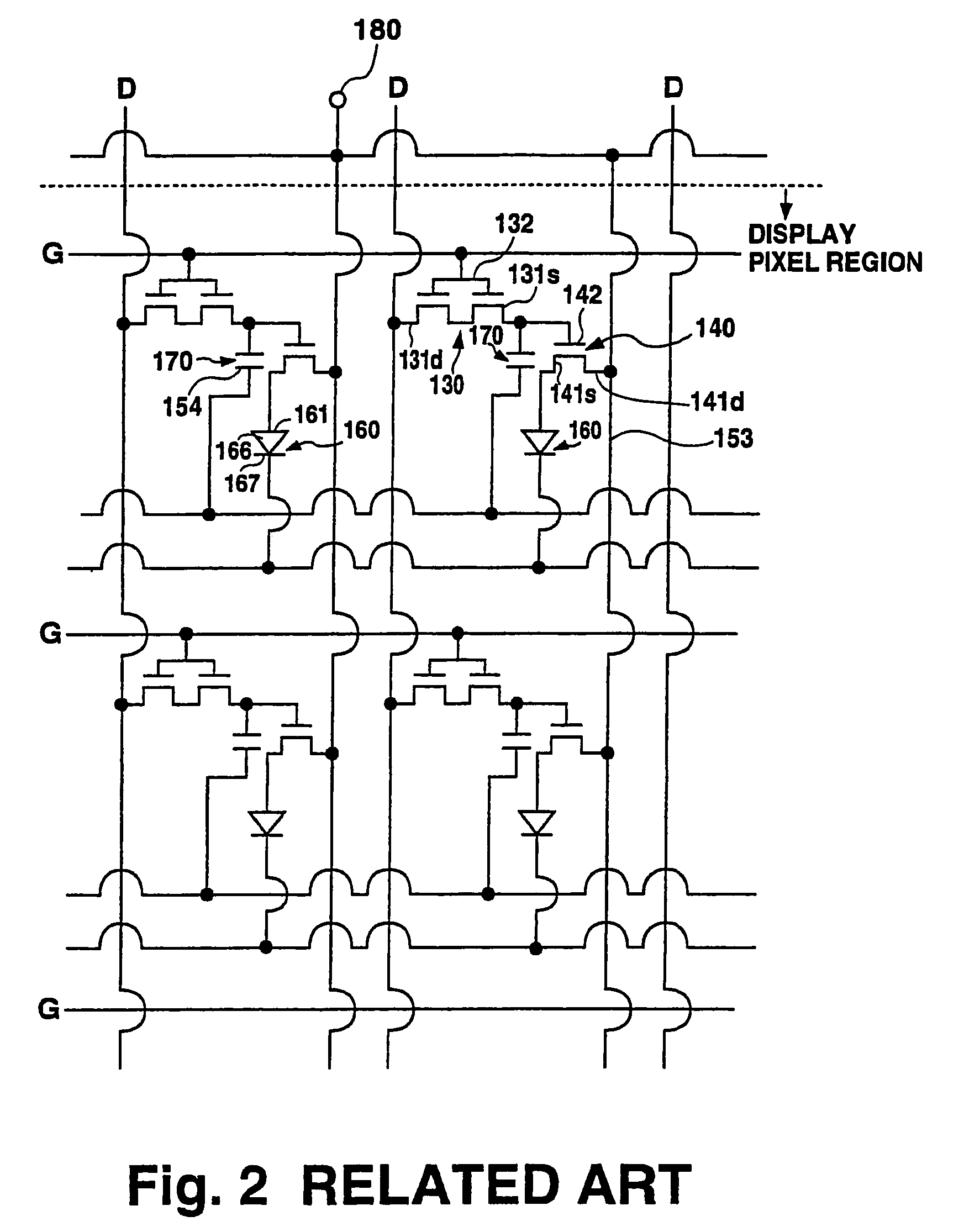
[0046]FIG. 4 is a plan view illustrating one display pixel in an organic EL display device implementing the present invention. FIG. 5 is a diagram showing an equivalent circuit for a plurality of display pixels of the organic EL display device. Each of FIGS. 6A and 6B shows a cross-sectional view taken along line B—B in FIG. 4. A separate drawing for the cross-sectional view taken along line A—A of FIG. 4 is not included because this view is identical to the previously described FIG. 3A.

[0047]In the present embodiment, TFTs having gate electrodes disposed underneath the active layer 131, namely, bottom-gate type TFTs, are employed as the first and second TFTs 130,140. The TFTs of the present embodiment use a p-Si film as the active layers, and include gate electrodes 132,142 comprising the double-gate structure.

[0048]The organic EL display device is configured by sequentially forming layers of TFTs and organic E...


PUM


Abstract

Power source lines (183) for supplying drive current from power source input terminals (180) to organic EL elements (160) formed in a display pixel region having display pixels are connected by a bypass line (181) along the row direction within the display pixel region. This arrangement minimizes decrease in power source current caused by resistance of the power source lines (183) according to the line length. Accordingly, the organic EL elements (160) can adequately receive the actual desired current, thereby achieving an organic EL device capable of bright displays and having uniform display luminance within the display region.

Description

CROSS-REFERENCE TO RELATED APPLICATION[0001]This application is a continuation of U.S. patent application Ser. No. 09 / 510,853, filed Feb. 23, 2000, now U.S. Pat. No. 6,724,149, the entire contents of which are incorporated herein by reference.BACKGROUND OF THE INVENTION[0002]1. Field of the Invention[0003]The present invention relates to an emissive display device using emissive elements, such as electroluminescence elements, which employs thin film transistors for controlling such elements.[0004]2. Description of the Related Art[0005]In recent years, electroluminescence (referred to hereinafter as “EL”) display devices comprising EL elements have gained attention as potential replacements for CRTs and LCDs. Research has been directed to the development of EL display devices using, for example, thin film transistors (referred to hereinafter as “TFT”) as switching elements to drive the EL elements.[0006]FIG. 1 is a plan view showing one display pixel of an organic EL display device. ...

Claims


Application Information

Patent Timeline
IPC IPC(8): G09G3/10H01L27/32
CPCH01L27/3276H10K59/131
Inventor KOMIYA, NAOAKIYOKOYAMA, RYOICHIYAMADA, TSUTOMUNISHIKAWA, RYUJI
Owner SANYO ELECTRIC CO LTD
Why Eureka
Try Eureka