
Diode and transistor design for high speed I/O

a high-speed i/o, diode technology, applied in the direction of diodes, semiconductor devices, semiconductor/solid-state device details, etc., can solve the problems of gate oxide breakdown, junction damage, and bus performance degradation

Inactive Publication Date: 2006-03-14
INTEL CORP
View PDF15 Cites 9 Cited by
  • Summary
  • Abstract
  • Description
  • Claims
  • Application Information

AI Technical Summary

Benefits of technology

[0017]An integrated circuit is disclosed. The integrated circuit includes a performance circuit occupying a first area of an integrated circuit substrate and a protection circuit coupled to the performan

Problems solved by technology

The larger the capacitance, the slower the charging or discharging, resulting in degraded bus performance.
If the voltage applied to the transistor becomes excessive, the gate oxide can break down, the junctions can be destroyed, and the metal to the transistor can be destroyed.
The main source of excessive high voltages to integrated circuits is triboelectricity.
If such a high voltage is applied to the pins of an integrated circuit package, its discharge, referred to as ElectroStatic Discharge (ESD), can cause breakdown of the devices to which the voltage is applied.
The breakdown event may cause sufficient damage to produce immediate destruction of the integrated circuit, or it may weaken the device enough that it will fail early in the operating life of the integrated circuit.
Since the breakdown mechanism is designed to be non-destructive, the circuits provide a normally open path that closes only when a high voltage appears at the input or output terminals, harmlessly discharging the node to which it is connected.
If the power is dissipated into too small a volume of silicon, the silicon can be heated beyond its melting point and the device destroyed.
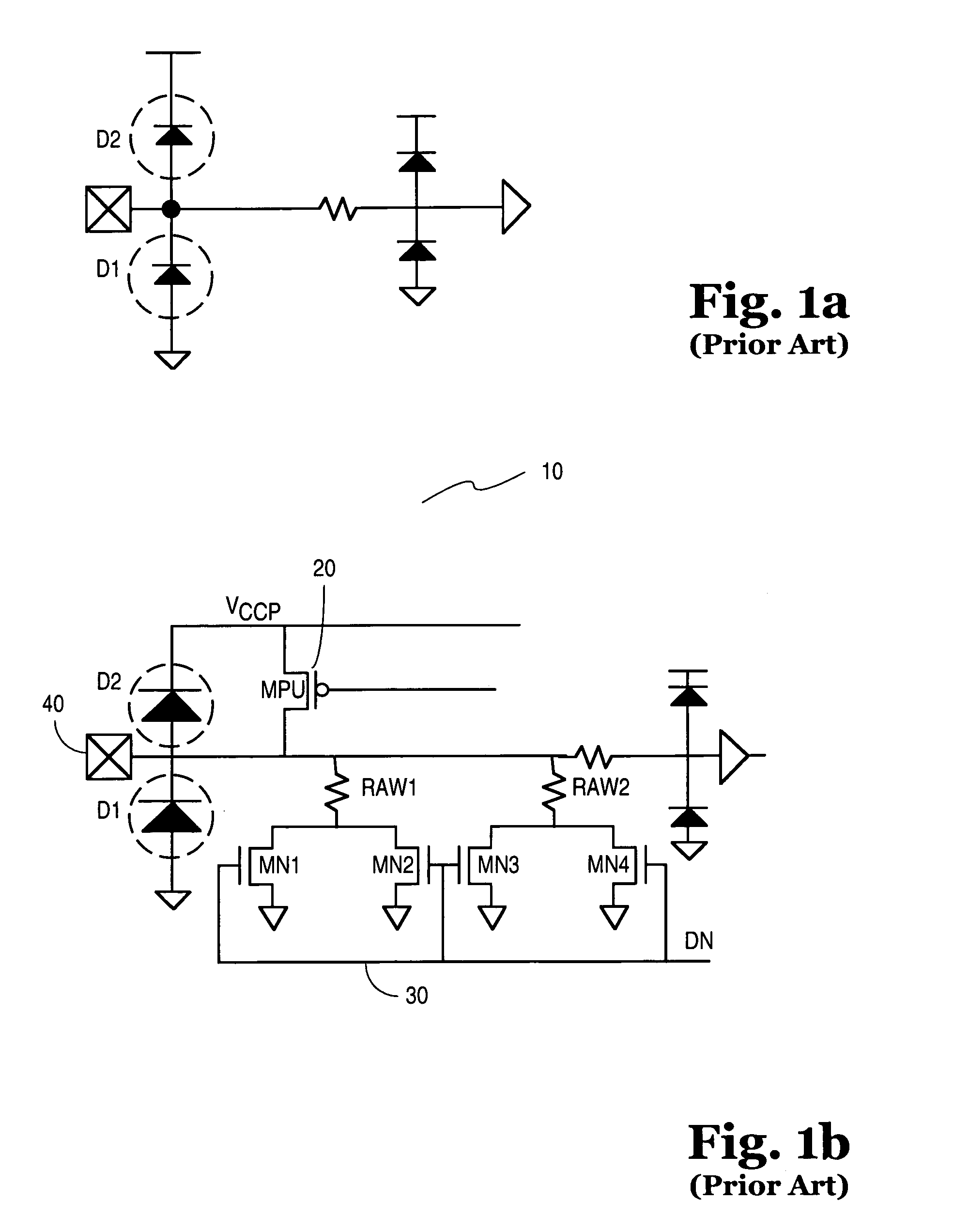
Therefore, D2 diode size is much larger than required resulting in extra capacitive loading.

Method used


Image

  • Diode and transistor design for high speed I/O
  • Diode and transistor design for high speed I/O
  • Diode and transistor design for high speed I/O

Examples


third embodiment

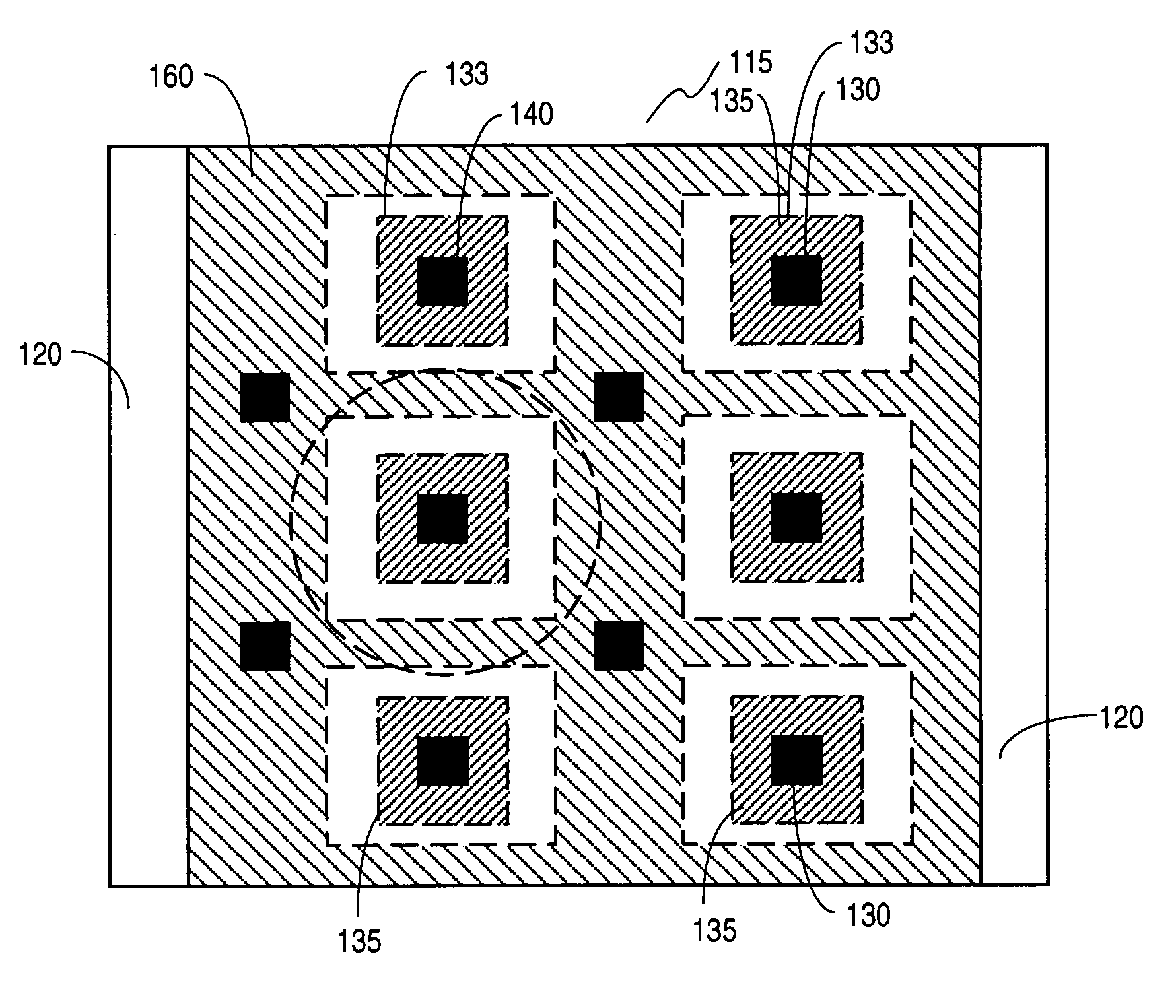
[0045]If higher current uniformity is desired, FIGS. 8 and 9 illustrate the partitioned protection circuit of the invention. In FIG. 8, unit cells 133 of p-type doped regions 133 are formed in n-well 120. p-type regions 160 are formed adjacent each edge of p-type units 133. In this manner, each unit cell 133 becomes an island in n-well 120 surrounded by n-type region 160. This surrounding of unit cell 133 with n-type region 160 is referred to herein as a “waffle” design.

[0046]FIG. 9 shows the current paths 165 from an edge of one unit cell 133 of FIG. 8. The current spreading improves the diode resistance over prior art diode structures. Resistance can be estimated and compared based on the length of the current path. Current path 165 has a trapezoidal shape, and the effective width of the path can be estimated as the average of the widths of the current source and sink. In FIG. 9, the current source has width “3S” and sink width “5S.” The diode resistance is reduced by current spre...

second embodiment

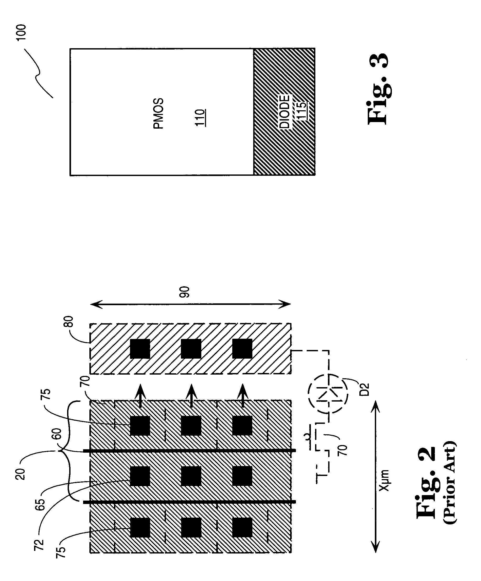
[0056]FIG. 12 shows a layout of the performance portion of the partitioned integrated circuit of the invention. In FIG. 12, individual unit cells 280 include a p-type doped region 285 and contact 290 in n-well 220. Here again, a unit cell is that minimum amount of p-typed doped area that will support a contact. Overlying and surrounding the periphery of unit cell 280 is polysilicon gate 295. In this case, p-type doped regions 285 of unit cells 280 serve as drain regions for the PMOS FET device. Surrounding drain region 285 of unit cells 280 is p-type source region 310. Summarizing the unit cell 280 structure as a waffle structure, one drain contact 290 serves four sides. Accordingly, the width to capacitance ratio is 4W / C, a gain of four times the width to capacitance ratio over prior art structures such as described in FIG. 2 and the accompanying text.

[0057]The waffle transistors described above can be analytically or empirically modeled similar to prior art “Ladder” transistors su...


PUM


Abstract

An integrated circuit including a performance circuit occupying a first area of an integrated circuit substrate and a protection circuit coupled to the performance circuit and occupying a second area of an integrated circuit substrate separate from the first area. Also, a method of forming an integrated circuit including the steps of: Forming a performance circuit occupying a first area of an integrated circuit substrate, forming a protection circuit occupying a second area of an integrated circuit separate from the first area, and coupling the protection circuit to the performance circuit.

Description

[0001]This is a divisional of application Ser. No. 09 / 107,351, filed Jun. 30, 1998, now U.S. Pat. No. 6,137,143.BACKGROUND OF THE INVENTION[0002]1. Field of the Invention[0003]The invention relates to integrated circuit devices and more particularly to layout techniques for such devices.[0004]2. Description of Related Art[0005]One area where parasitic capacitance is noted is in input / output (I / O) buffer circuits. For high speed I / O circuits, the parasitic capacitance is one limiter to the fast transitioning edges of the circuit. The larger the capacitance, the slower the charging or discharging, resulting in degraded bus performance. Thus, many efforts have been put forth to reduce the capacitive load and create faster transitions which in turn leads to faster I / O circuits.[0006]The input signals to an integrated circuit, for example, a metal oxide semiconductor (MOS) integrated circuit, are generally fed to transistors. If the voltage applied to the transistor becomes excessive, th...

Claims


Application Information

Patent Timeline
IPC IPC(8): H01L23/62H01L27/02
CPCH01L27/0255H01L2924/0002H01L2924/00
Inventor DABRAL, SANJAYSESHAN, KRISHNA
Owner INTEL CORP
Learn More