Coaxial waveguide microstructures and methods of formation thereof

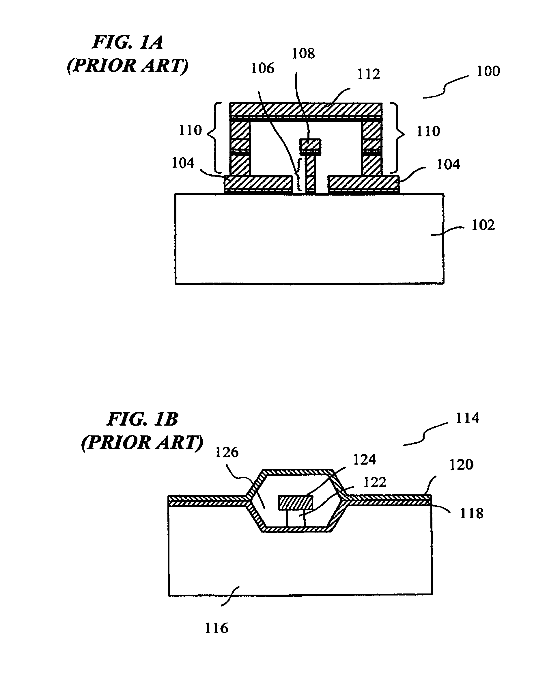
a microstructure and waveguide technology, applied in waveguides, waveguide types, insulation conductors/cables, etc., can solve the problems of coaxial waveguide structure, create signal interference, and process is not readily scalable to a stacked structure having a plurality of coaxial layer structures

Active Publication Date: 2006-03-14
CUBIC CORPORATION
View PDF9 Cites 382 Cited by
  • Summary
  • Abstract
  • Description
  • Claims
  • Application Information

AI Technical Summary

Benefits of technology

[0007]In accordance with a first aspect of the invention, provided are coaxial waveguide microstructures. The microstructures include a substrate and a coaxial waveguide disposed above the substrate. The coaxial waveguide includes: a center conductor; an outer conductor including one or more walls, spaced apart from and disposed around the center conductor; one or more dielectric support members for supporting the center conductor in contact with the center conductor and enclosed within the outer conductor; and a core volume between the center conductor and the outer conductor, wherein the core volume is under vacuum or in a gas state.

Problems solved by technology

There are various disadvantages associated with this type of coaxial waveguide structure.
For example, the use of metal supporters for supporting the signal line would result in some degree of reflection of the propagated waves and thus create signal interference.
Further, the process is not readily scalable to a stacked structure having a plurality of coaxial layer structures due, for example, to the requirement that the metal supporters be connected to the dielectric substrate as a means of support.
In addition, the choice of a substrate material in this known structure is not flexible, but is limited to dielectric materials to achieve similar waveguiding performance.
Further, the coaxial waveguide structure cannot be separated from the substrate due to the requisite mechanical connection of the supporters to the substrate.
For example, the process is not sealable to a multiple coaxial layer structure due to the requirement of a recessed substrate, the geometry of the waveguide structure, and the requirement for a groove on a planar substrate to achieve the requisite planarization.

Method used


Image

  • Coaxial waveguide microstructures and methods of formation thereof
  • Coaxial waveguide microstructures and methods of formation thereof
  • Coaxial waveguide microstructures and methods of formation thereof

Examples


Embodiment Construction

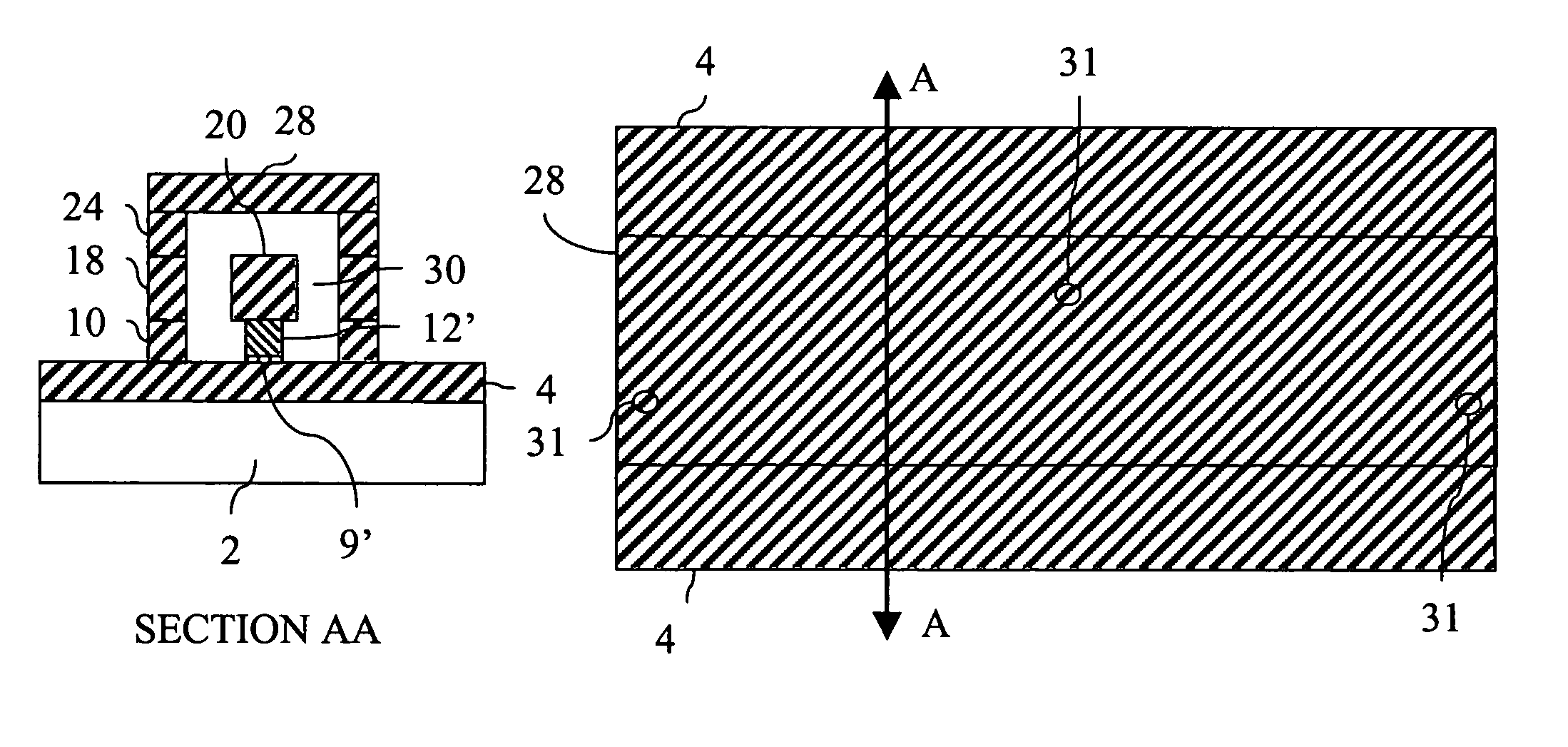
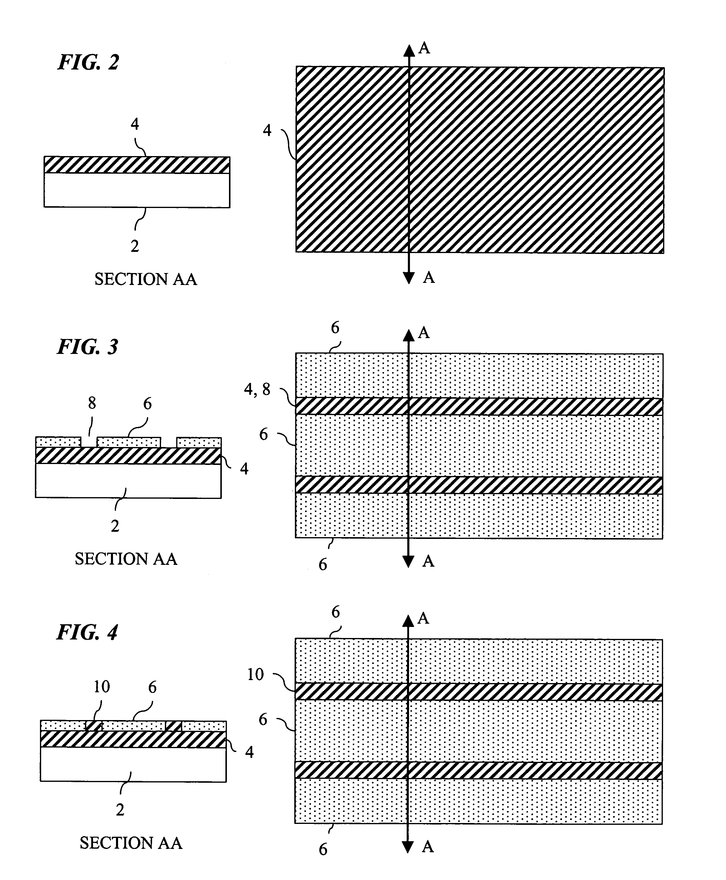
[0022]The exemplary processes to be described involve a sequential build to create microstructures containing metal, dielectric and gas or a vacuous atmosphere. In the sequential build process, a structure is formed by sequentially layering various materials in a defined manner. When implemented with lithographic patterning and other optional processes, for example, planarization techniques, a flexible method to form a variety of components, such as the exemplified suspended coaxial waveguide microstructures, is provided.

[0023]The sequential build process is generally accomplished through processes including one or more of: (a) metal coating, sacrificial photoresist coating, and dielectric coating processes; (b) surface planarization; (c) photolithography; and (d) etching or other layer removal processes. In depositing metal, plating techniques have been found to be particularly useful, although other metal deposition techniques such as physical vapor deposition (PVD) and chemical v...


PUM

PropertyMeasurementUnit
thicknessaaaaaaaaaa
skin depthaaaaaaaaaa
thicknessaaaaaaaaaa

Abstract

Provided are coaxial waveguide microstructures. The microstructures include a substrate and a coaxial waveguide disposed above the substrate. The coaxial waveguide includes: a center conductor; an outer conductor including one or more walls, spaced apart from and disposed around the center conductor; one or more dielectric support members for supporting the center conductor in contact with the center conductor and enclosed within the outer conductor; and a core volume between the center conductor and the outer conductor, wherein the core volume is under vacuum or in a gas state. Also provided are methods of forming coaxial waveguide microstructures by a sequential build process and hermetic packages which include a coaxial waveguide microstructure.

Description

CROSS-REFERENCE TO RELATED APPLICATIONS[0001]This application claims the benefit of priority under 35 U.S.C. §119(e) to U.S. Provisional Application Nos. 60 / 452,073 filed Mar. 4, 2003, and 60 / 474,549 filed May 29, 2003, the entire contents of which applications are incorporated herein by reference.GOVERNMENT INTEREST[0002]This invention was made with Government support under Agreement No. W911QX-04-C-0097 awarded by DARPA. The Government has certain rights in the invention.FIELD OF THE INVENTION[0003]This invention relates generally to microfabrication technology and to electronic devices. More particularly, the present invention relates to coaxial waveguide microstructures and to methods of forming such microstructures, as well as to electronic devices which include such microstructures.BACKGROUND OF THE INVENTION[0004]Coaxial waveguide microstructures formed by sequential build processes have been described, for example, in International Application Publication No. WO 00 / 39854 (WO...

Claims


Application Information

Patent Timeline
Patent Type & Authority Patents(United States)
IPC IPC(8): H01P3/06H01P11/00H05K1/02H05K3/46
CPCH01P1/08H01P3/06H01P5/103H01P11/002H01P11/003H01P11/005H01P3/00H05K1/0221Y10T29/49117H05K1/0272H05K3/4644H05K3/4685H05K2201/09809Y10T29/49123H01P5/183
Inventor SHERRER, DAVID W.FISHER, JOHN J.
Owner CUBIC CORPORATION
Why Eureka
Try Eureka