Probe card for testing semiconductor device

a technology for semiconductor devices and probe cards, which is applied in the direction of individual semiconductor device testing, coupling device connection, instruments, etc., can solve the problems of affecting the reliability of the main board, the flexibility of the connection between the main board and the sub board, and the damage to the welded or soldered part of the circuit board, etc., to enhance the stability of high-frequency signal transmission efficiency, improve assembly characteristics, and widen the range of effects

Inactive Publication Date: 2006-03-21
YULIM HITECH
View PDF6 Cites 120 Cited by
  • Summary
  • Abstract
  • Description
  • Claims
  • Application Information

AI Technical Summary

Benefits of technology

[0021]It is therefore an object of the present invention to provide a probe card for testing a semiconductor devices that has flexibility in a wide range for an elastic connection between a main board and a sub board and provides an improved assembly characteristic to enhance a stable high-frequency signal transmission efficiency and guarantee a readiness of fabrication.
[0022]It is another object of the present invention to provide a probe card for testing a semiconductor devices that achieves a terminal connection between the boards through elastic connection pins to achieve a stable connection and a reduced contact shock and thereby provide a strong connection structure.
[0023]It is still another object of the present invention to provide an improved needle tip having a firm and constant connection area and thereby to guarantee a more stable connection.

Problems solved by technology

In other words, the most important real problem in the technological development of the probe card is appropriately coping with the testing of semiconductor devices that are fabricated in a larger number with its miniaturization from a larger wafer, and testing a larger number of semiconductor devices in a simultaneous manner.
However, the conventional interface means for transmission of electrical signals between the main board and the sub board has no or little connection flexibility.
Such an interface means has no flexibility at all, so a vertical impact due to the contact with the connection terminals of the semiconductor device in use may cause damages on the welded or soldered part of the circuit board, particularly damaging the main board that is a relatively expensive component part.
Once the main board, the interface means, and the sub board are combined together firmed by welding or soldering, they cannot be separated from one another, causing an uneconomical problem in regard to the difficulty of repair.
The flatness of the sub board is of a great importance in achieving a stable connection, but there is no configuration for guaranteeing the flatness.
With a defective detected in the testing in the assembly situation, there is no way but do away with the probe card due to the difficulty of disassembly and repair, causing a great economic loss.

Method used


Image

  • Probe card for testing semiconductor device
  • Probe card for testing semiconductor device
  • Probe card for testing semiconductor device

Examples


Embodiment Construction

[0031]In the following detailed description, only the preferred embodiment of the invention has been shown and described, simply by way of illustration of the best mode contemplated by the inventor(s) of carrying out the invention. As will be realized, the invention is capable of modification in various obvious respects, all without departing from the invention. Accordingly, the drawings and description are to be regarded as illustrative in nature, and not restrictive. To clarify the present invention, parts not described in the specification are omitted.

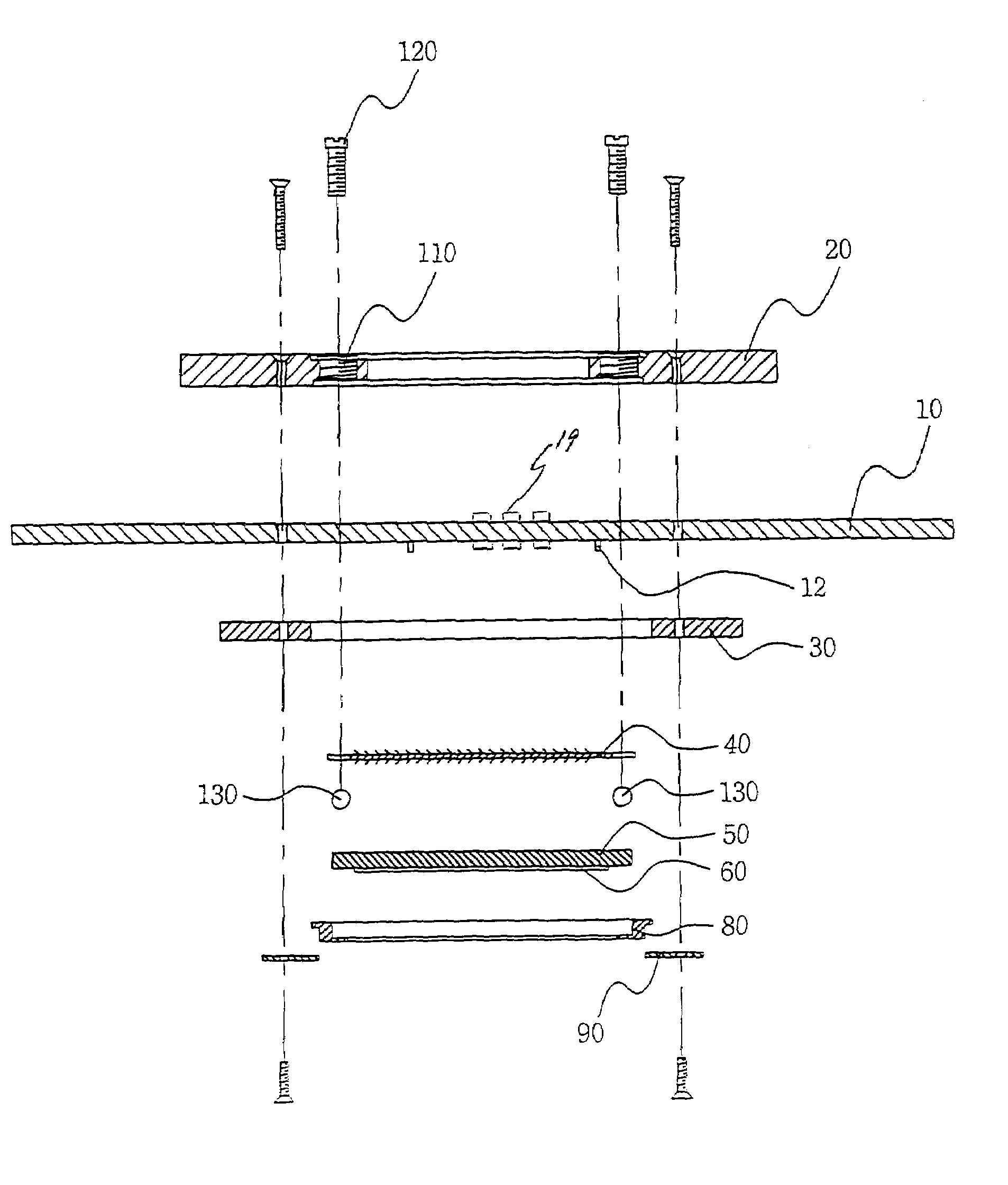
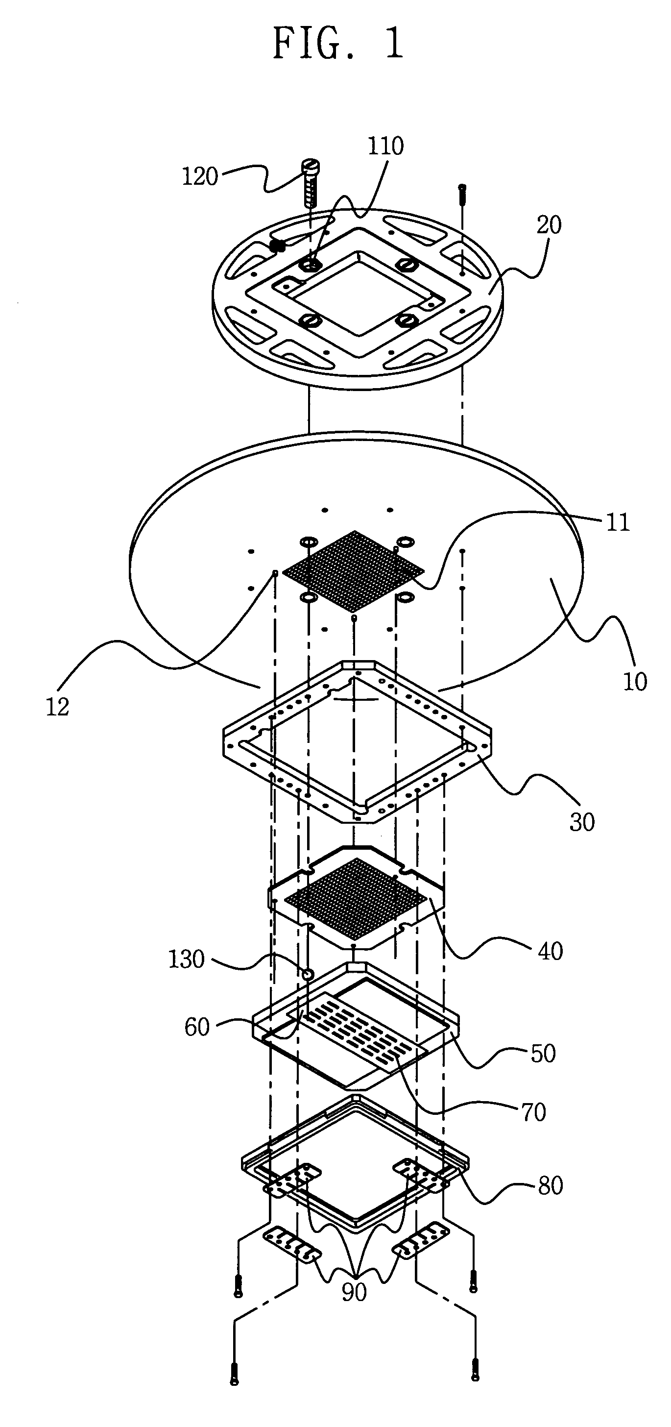
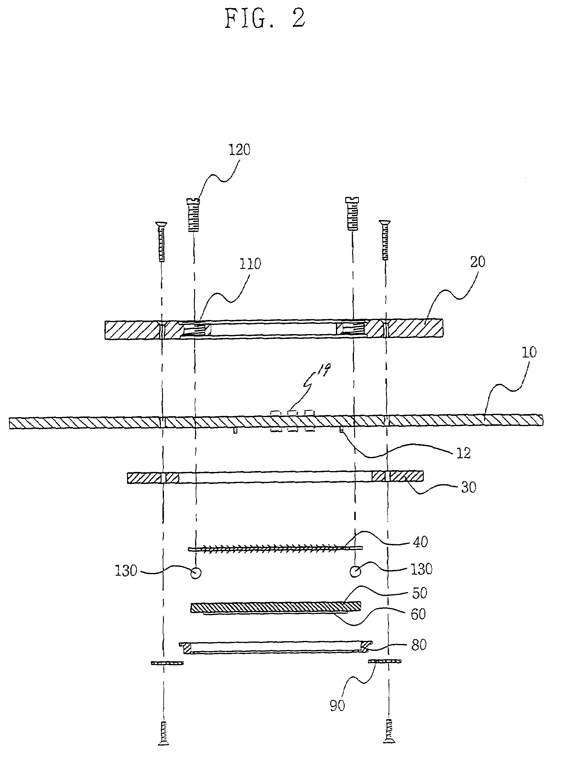
[0032]FIG. 1 is a perspective view of a disassembled probe card for testing semiconductors according to the present invention, and FIG. 2 is an exploded cross-section of the probe card of the present invention.

[0033]The probe card of the present invention comprises, as shown in FIGS. 1 and 2, a main board member 10, an upper reinforcing plate 20, a lower reinforcing plate 30, an interface member 40, a sub board member 50, a needle g...


PUM


Abstract

A probe card for testing semiconductor devices includes a main board member, an upper reinforcing plate, a lower reinforcing plate, an interface member, a sub board member, a needle guide member, a needle member, a side cover member, and a clamping member. The probe card achieves an interface between the circuit boards through elastic connection pins so as to cope with a connection shock with the connection terminals of a semiconductor device, thereby preventing damages on the boards, and has the component parts combined together simply by face contacts to facilitate assembly and disassembly of the component parts and thereby to provide a great economical advantage in the aspect of maintenance and repair.

Description

PRIORITY[0001]This application claims priority to an application entitled “Probe Card for Testing Semiconductor” filed in the Korean Industrial Property Office on Jul. 5, 2004 and assigned Serial No. 2004-51988, and to an application entitled “Probe Card for Testing Semiconductor” filed in the Korean Industrial Property Office on Oct. 14, 2004 and assigned Serial No. 2004-82020, the contents of both of which are incorporated herein by reference.BACKGROUND OF THE INVENTION[0002]1. The Field of the Invention[0003]This invention relates to a probe card for testing semiconductor devices. More particularly, this invention relates to a probe card for testing semiconductor devices that has a simplified circuit configuration for internal transmission of electrical signals and enhances its fabrication and assembly characteristics to guarantee improved reliability to productivity and performance.[0004]2. Description of the Related Art[0005]Generally, the process for manufacturing a semiconduc...

Claims


Application Information

Patent Timeline
Patent Type & Authority Patents(United States)
IPC IPC(8): H01R11/18
CPCG01R1/07378
Inventor YOON, SOO
Owner YULIM HITECH
Why Eureka
Try Eureka