Method and system for calibrating a laser processing system and laser marking system utilizing same

a laser processing system and laser marking technology, applied in the field of method and system for calibrating a laser processing system and laser marking system utilizing same, can solve problems such as poor mark quality or mark positioning errors

Inactive Publication Date: 2006-03-21
ELECTRO SCI IND INC
View PDF61 Cites 145 Cited by
  • Summary
  • Abstract
  • Description
  • Claims
  • Application Information

AI Technical Summary

Benefits of technology

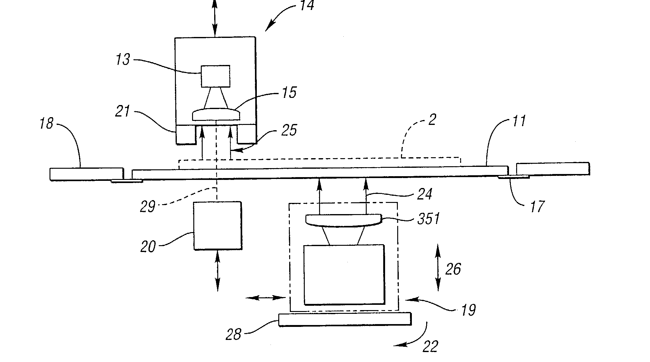
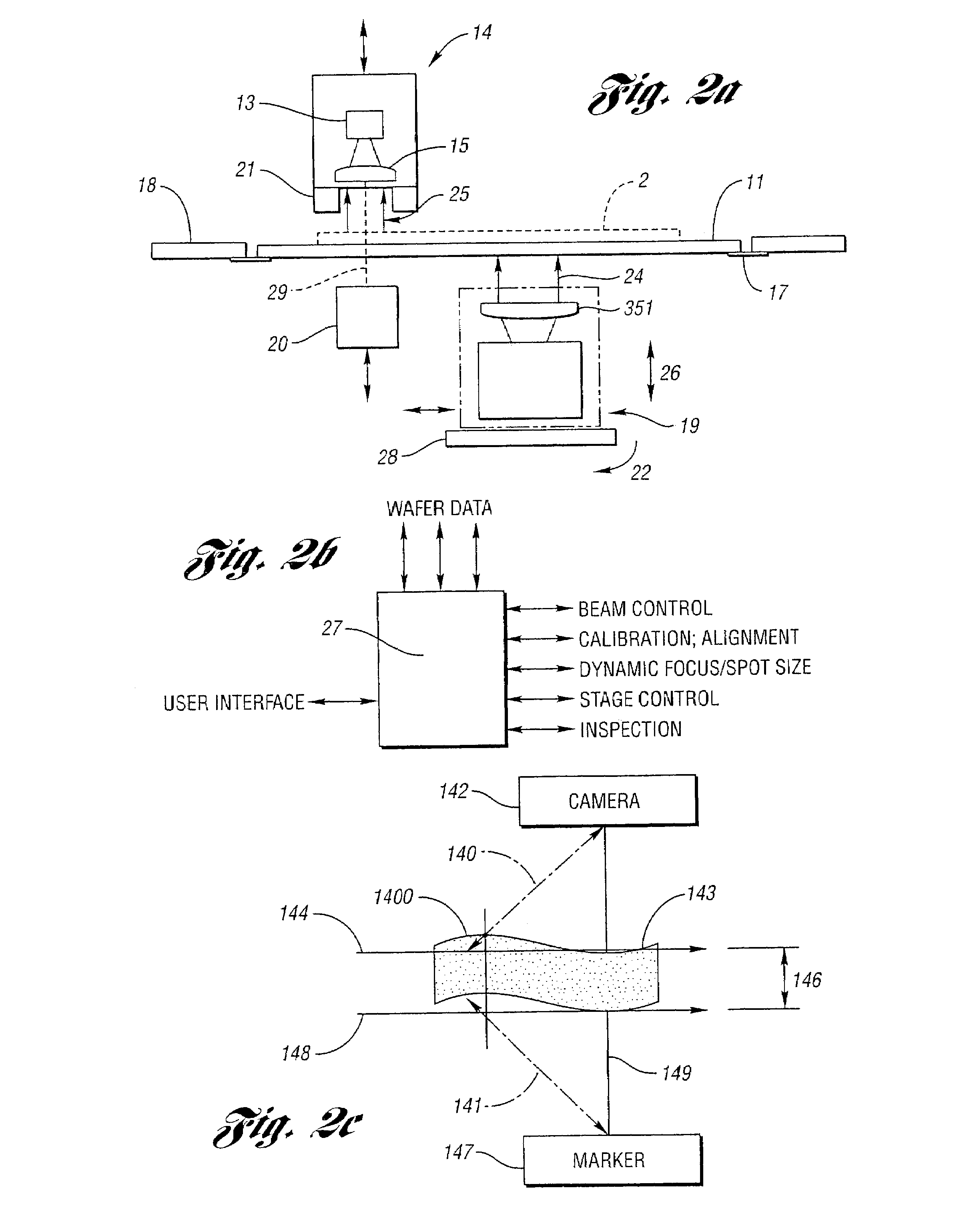
[0018]Still further in carrying out the above object and other objects of the present invention, a laser-based wafer marking system is provided for marking a wafer having a topside containing a circuit. The circuit has circuit features and the wafer has a backside to be marked. The system includes a calibrated galvanometer marking head having a scan lens and a marking field substantially smaller than the wafer. The system further includes a calibrated positioning stage for carrying the wafer with a range of motion large enough to position any wafer location to be marked to within the marking field. The system still further includes a calibrated alignment camera with a field of view substantially smaller than the wafer. A frame mounts the stage rigidly with respect to the camera and the marking head. A controller has a map for coordinating locations of the marking head, the stage and the alignment camera for causing the stage and the marking head to be positioned relative to each other such that the wafer is accurately marked on its backside relative to the circuit features on the front side.

Problems solved by technology

Tolerance stackups within the system and workpiece may lead to poor mark quality or mark positioning errors.

Method used


Image

  • Method and system for calibrating a laser processing system and laser marking system utilizing same
  • Method and system for calibrating a laser processing system and laser marking system utilizing same
  • Method and system for calibrating a laser processing system and laser marking system utilizing same

Examples


Embodiment Construction

Overview

[0060]Several components of a system 100 for laser marking and inspection of wafers, for instance 300 mm wafers, is schematically illustrated in FIG. 5A. A robot 101 transfers a wafer from a FOUP (Front Opening Unified Portal) delivery device to a pre-aligner 102 which is used to find the notch or flat of the wafer so as to orient the wafer for further processing. Reader 103 may be used to extract certain coded information which in turn may be used in subsequent processing steps. A precision stage 104 is used, and a fine alignment procedure included to correct the residual error of the pre-aligner (e.g., X, Y, rotation). The wafer is marked. All marks, or a designated subset, are then inspected. In the arrangement of FIG. 5A the inspection system is used with a separate inspection stage 105.

[0061]A marking sequence, following opening of a FOUP, includes:[0062]1. Robot moves the wafer to the pre-aligner and establishes a notch-die positional relation.[0063]2. The wafer ID is ...


PUM

PropertyMeasurementUnit
thicknessaaaaaaaaaa
thicknessaaaaaaaaaa
diameteraaaaaaaaaa

Abstract

A method of calibrating a laser marking system includes calibrating a laser marking system in three dimensions. The step of calibrating includes storing data corresponding to a plurality of heights. A position measurement of a workpiece is obtained to be marked. Stored calibration data is associated with the position measurement. A method and system for calibrating a laser processing or marking system is provided. The method includes: calibrating a laser marker over a marking field; obtaining a position measurement of a workpiece to be marked; associating stored calibration data with the position measurement; relatively positioning a marking beam and the workpiece based on at least the associated calibration data; and calibrating a laser marking system in at least three degrees of freedom. The step of calibrating includes storing data corresponding to a plurality of positions and controllably and relatively positioning a marking beam based on the stored data corresponding to the plurality of positions.

Description

CROSS-REFERENCE TO RELATED APPLICATION[0001]This application claims the benefit of U.S. provisional application Ser. No. 60 / 381,602, filed May 17, 2002.BACKGROUND OF THE INVENTION[0002]1. Field of the Invention[0003]The invention relates to calibration of laser-based workpiece micromachining and similar material processing systems, wherein the work-piece has considerable warpage or sag. The workpiece may be a semiconductor wafer, for instance a 300 mm wafer, with a thickness of a few hundred microns.[0004]2. Background Art[0005]The following representative patent references relate to various aspects of laser marking of wafers and electronic assemblies, illumination, and inspection / reading marks: U.S. Pat. Nos. 4,522,656; 4,945,204; 5,329,090; 6,309,943; 6,262,388; 5,929,997; 5,690,846; 5,894,530; 5,737,122; and Japanese Patent Abstract 11135390.[0006]The following representative references provide general information on various laser marking methods and system configurations and com...

Claims


Application Information

Patent Timeline
Patent Type & Authority Patents(United States)
IPC IPC(8): B23K26/00B23K26/02B23K26/03B23K26/04B23K26/08B23K26/36B41M5/24G06K1/12H01C17/242H01L21/00H01L21/02H01L21/68H01L23/544
CPCB23K26/04B23K26/043B23K26/0853B23K26/365B23K26/4075G06K1/126H01L21/67282H01L21/681H01L23/544B23K26/426B23K26/041B23K2201/007B23K2201/40H01C17/242H01L2223/5442H01L2223/54453H01L2223/54473H01L2223/5448B23K26/40B23K26/042B23K26/361B23K26/705B23K2101/007B23K2101/40B23K2103/50H01L2924/0002H01L2924/00B23K26/02
Inventor CAHILL, STEVEN P.EHRMANN, JONATHAN S.LI, YOU C.SCHRAMM, RAINERPELSUE, KURT
Owner ELECTRO SCI IND INC
Why Eureka
Try Eureka