Back-side-of-die, through-wafer guided-wave optical clock distribution networks, method of fabrication thereof, and uses thereof

Inactive Publication Date: 2006-03-21
GEORGIA TECH RES CORP
View PDF23 Cites 231 Cited by
  • Summary
  • Abstract
  • Description
  • Claims
  • Application Information

AI Technical Summary

Problems solved by technology

However, current clock distribution networks suffer from unknown (or unpredictable) components of global and local skew and jitter.
Such distribution systems may address only a limited portion of the timing uncertainty associated with global and semi-global levels of electrical wiring and clock drivers, as the varying path length and internal scattering may contribute additional skew and jitter tha

Method used


Image

  • Back-side-of-die, through-wafer guided-wave optical clock distribution networks, method of fabrication thereof, and uses thereof
  • Back-side-of-die, through-wafer guided-wave optical clock distribution networks, method of fabrication thereof, and uses thereof
  • Back-side-of-die, through-wafer guided-wave optical clock distribution networks, method of fabrication thereof, and uses thereof

Examples


example 1

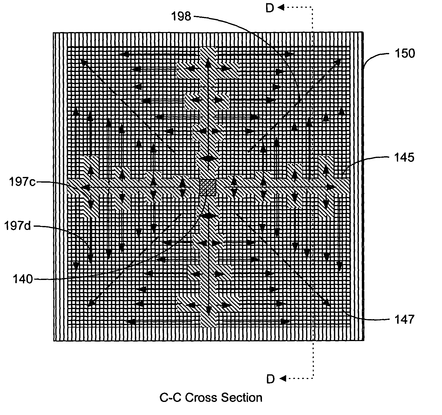
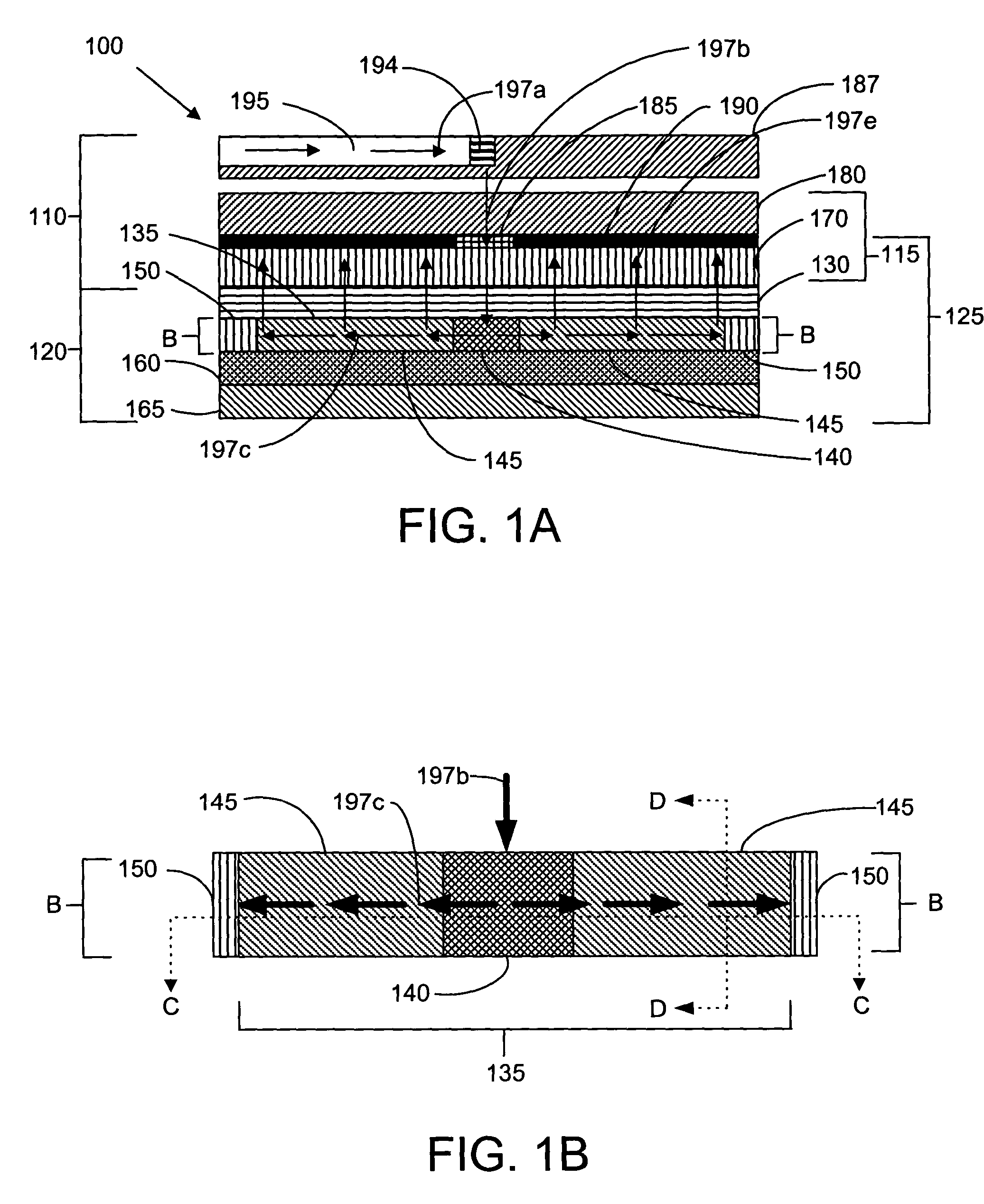
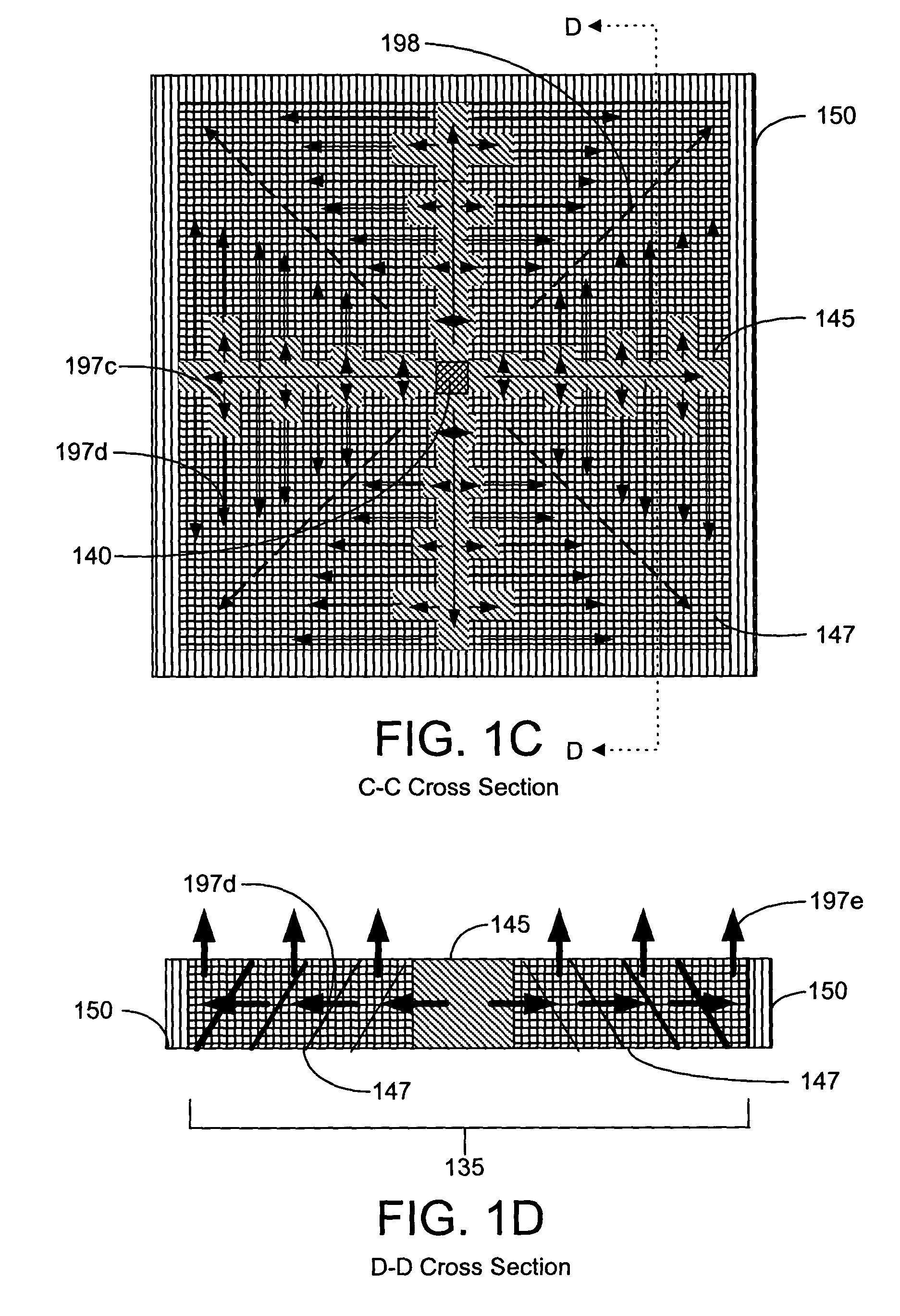
[0029]FIG. 1A is a cross-sectional view of a representative embodiment of a back-side-of-die, through-wafer guided-wave optical clock distribution system (network) 100 with off-chip optical clock signal generation, where no on-chip routing of the optical signal occurs prior to coupling the signal to the back-side-of-die core layer from an off-chip optical source. The back-side-of-die, through-wafer guided-wave optical clock distribution system 100 includes front-side layers 110 and back-side layers 120. The front-side layers 110 include, but are not limited to, a device substrate 170, a packaging layer 180, a printed wiring board substrate 187, an optical via 185, and device circuitry 190. The back-side layers 120 include, but are not limited to, a first cladding layer 130, a core layer 135, a horizontal reflection absorption layer 150, a second cladding layer 160, and a vertical reflection absorption layer 165. The core layer 135 includes, but is not limited to, multiplexed vertica...

example 2

[0058]FIG. 2 is a cross-sectional view of another representative embodiment of a back-side-of-die, through-wafer guided-wave optical clock distribution system 200 with off-chip optical clock signal generation, where chip-level distribution of the optical clock signal occurs prior to coupling the signal to the back-side-of-die core layer.

[0059]The back-side-of-die, through-wafer guided-wave optical clock distribution system 200 includes, but is not limited to, front-side layers 210 and back-side layers 220. The front-side layers 210 include, but are not limited to, a device substrate 270, a packaging layer 280, a printed wiring board substrate 287, an optical via 285, and device circuitry 290. The back-side layers 220 include, but are not limited to, a first cladding layer 230, a core layer 235, a horizontal reflection absorption layer 250, a second cladding layer 260, and a vertical reflection absorption layer 265. The core layer 235 includes, but is not limited to, a vertical-to-ho...

example 3

[0063]FIG. 3 is a cross-sectional view of yet another representative embodiment of a back-side-of-die, through-wafer guided-wave optical clock distribution system 300 with on-chip optical clock signal generation.

[0064]The back-side-of-die, through-wafer guided-wave optical clock distribution system 300 includes front-side layers 310 and back-side layers 320. The front-side layers 310 include, but are not limited to, a device substrate 370, a packaging layer 380, a printed wiring board substrate 387, an optical source 399, and device circuitry 390. The back-side layers 320 include, but are not limited to, a first cladding layer 330, a core layer 335, a horizontal reflection absorption layer 350, a second cladding layer 360, and a vertical reflection absorption layer 365. The core layer 335 includes, but is not limited to, a vertical-to-horizontal input diffraction grating 340, a horizontal-to-horizontal diffraction grating 345, and a horizontal-to-vertical output diffraction grating ...


PUM


Abstract

Systems and methods for back-of-die, through-wafer guided-wave optical clock distribution systems (networks) are disclosed. A representative back-of-die, through-wafer guided-wave optical clock distribution system includes an integrated circuit device with a first cladding layer disposed on the back-side of the integrated circuit device, and an core layer disposed on the first cladding layer. The core layer, the first cladding layer, or the second cladding layer can include, but is not limited to, vertical-to-horizontal input diffraction gratings, a horizontal-to-horizontal diffraction gratings, and horizontal-to-vertical output diffraction gratings.

Description

CROSS-REFERENCE TO RELATED APPLICATION[0001]This application claims priority to U.S. provisional application entitled, “UNFUOCUSED GUIDED-WAVE OPTICAL CLOCK DISTRIBUTION NETWORK AND METHOD,” having Ser. No. 60 / 399,975, filed on Jul. 31, 2002, which is entirely incorporated herein by reference.STATEMENT REGARDING FEDERALLY SPONSORED RESEARCH OR DEVELOPMENT[0002]The U.S. government may have a paid-up license in this invention and the right in limited circumstances to require the patent owner to license others on reasonable terms as provided for by the terms of MDA972-99-1-0002 awarded by the DARPA.TECHNICAL FIELD[0003]The present invention is generally related to clock distribution networks and more particularly, the present invention is related to guided-wave optical clock distribution networks employing a back-side-of-die core layer that communicates with optical sources through the device substrate upon which it resides, methods of fabricating back-side-of-die guided-wave optical c...

Claims


Application Information

Patent Timeline
IPC IPC(8): G02B6/34G02B6/12G02B6/124G02B6/43
CPCG02B6/12002G02B6/43G02B6/34G02B6/124
Inventor MULE, TONYMEINDL, JAMES D.GAYLORD, THOMAS K.
Owner GEORGIA TECH RES CORP
Why Eureka
Try Eureka