Photoelectric conversion device and manufacturing method thereof

a technology of conversion device and photoelectric technology, which is applied in the direction of color television, radio control device, television system, etc., can solve the problems of limited shape of the interlayer lens based on the shape of the pattern, and limited curved surface formed in the insulating film that forms the interlayer lens, so as to improve light condensation efficiency and reduce sensitivity

Inactive Publication Date: 2006-03-28
CANON KK
View PDF16 Cites 44 Cited by
  • Summary
  • Abstract
  • Description
  • Claims
  • Application Information

AI Technical Summary

Benefits of technology

[0014]Accordingly, an object of the present invention is to provide a photoelectric conversion device and a manufacturing method thereof, the photoelectric conversion device having interlayer lenses and being capable of improving the light condensation efficiency without substantially decreasing the sensitivity.
[0016]Since the upward convex-shaped interlayer lens may be formed to have a desired convex shape regardless of the shapes of an insulating film and / or a pattern formed thereunder, by appropriately setting the curvature, thickness, and the like of the convex shape of the interlayer lens, the light condensation efficiency of the interlayer lens can be improved, and in particular, the structure described above may be effectively applied to a photoelectric conversion device having a plurality of wire layers.
[0018]According to the method for manufacturing a photoelectric conversion device, of the present invention, a photoelectric conversion device can be manufactured having interlayer lenses which can improve the light condensation efficiency without substantially decreasing the sensitivity.

Problems solved by technology

However, according to the manufacturing method depicted in FIG. 11, a curved surface formed in the insulating film that forms the interlayer lenses is limited to having “peaks” above constituent elements of the pattern (e.g., 203) and “valleys” therebetween.
Thus, the shape of the interlayer lens depends on the shape of the pattern and is also limited thereby.

Method used


Image

  • Photoelectric conversion device and manufacturing method thereof
  • Photoelectric conversion device and manufacturing method thereof
  • Photoelectric conversion device and manufacturing method thereof

Examples


first embodiment

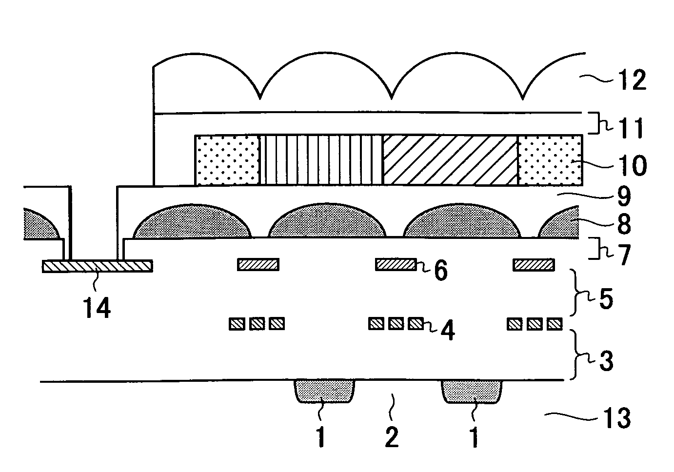
[0035]FIG. 1 is a schematic cross-sectional view of a photoelectric conversion device of a first embodiment according to the present invention.

[0036]As shown in FIG. 1, in the photoelectric conversion device of this embodiment, photoelectric conversion elements 1 are formed along a surface of a semiconductor member 13, and an element isolation region 2 is provided between adjacent photoelectric conversion elements 1. In addition, on the semiconductor member 13, a first insulating film 3 is provided. On the first insulating film 3, a first pattern 4 provided above the element isolation region 2, a second insulating film 5 covering the first pattern 4, a second pattern 6 provided above the element isolation region 2 and the first pattern 4, and a third insulating film 7 covering the second pattern 6 are formed in that order. In addition, on the third insulating film 7, upward convex-shaped interlayer lenses 8 are formed, the peak of each upward convex shape projecting in the direction...

second embodiment

[0062]FIG. 6 is a schematic cross-sectional view of a photoelectric conversion device according to a second embodiment of the present invention.

[0063]As shown in FIG. 6, in the photoelectric conversion device of this embodiment, the photoelectric conversion elements 1 are formed along a surface of the semiconductor member 13, and the element isolation region 2 is provided between adjacent photoelectric conversion elements 1. The first insulating film 3 is formed on the semiconductor member 13. On the first insulating film 3, the first pattern 4 disposed above the element isolation region 2, the second insulating film 5 covering the first pattern 4, and the second pattern 6 disposed above the element isolation region 2 and the first pattern 4 are formed in that order. In addition, on the second insulating film 5 and the second pattern 6, the upward convex-shaped interlayer lenses 8 are provided, the peak of each convex shape projecting in a direction from the photoelectric conversion...

third embodiment

[0085]FIG. 12 is a schematic cross-sectional view of a photoelectric conversion device according to a third embodiment of the present invention. In this figure, the same reference numerals as those in the first and the second embodiments designate constituent elements having the same functions, and detailed descriptions thereof will be omitted.

[0086]As shown in FIG. 12, in the photoelectric conversion device of this embodiment, three layers (first, second, and third patterns 124, 126, and 128) of patterns (wire layers) are formed above the photoelectric conversion elements, and on the photoelectric conversion elements, a first insulating layer 123, the first pattern 124, a second insulating layer 125, the second pattern 126, a third insulating layer 127, the third pattern 128, and a fourth insulating layer 129 are formed in that order. The surfaces of the individual insulating layers are preferably planarized by CMP or the like.

[0087]In the topmost wire layer 128, the pad portion 14...


PUM


Abstract

A photoelectric conversion device is provided which is capable of improving the light condensation efficiency without substantially decreasing the sensitivity. The photoelectric conversion device has a first pattern provided above an element isolation region formed between adjacent two photoelectric conversion elements, a second pattern provided above the element isolation region and above the first pattern, and microlenses provided above the photoelectric conversion elements with the first and the second patterns provided therebetween. The photoelectric conversion device further has convex-shaped interlayer lenses in optical paths between the photoelectric conversion elements and the microlenses, the peak of each convex shape projecting in the direction from the electro-optical element to the microlens.

Description

BACKGROUND OF THE INVENTION[0001]1. Field of the Invention[0002]The present invention relates to photoelectric conversion devices and manufacturing methods thereof, the devices used for image input apparatuses such as digital cameras, video cameras, and image readers.[0003]2. Description of the Related Art[0004]In recent years, photoelectric conversion devices have been incorporated in image input apparatuses such as digital cameras, video cameras, and image readers. These photoelectric conversion devices include, for example, CCD image sensors and non-CCD image sensors, such as bipolar transistor image sensors, field effect transistor image sensor, and CMOS image sensors. In such photoelectric conversion devices, optical image information is converted into electrical signals, which are processed using various types of signal processing and displayed in a display device or recorded on a recording medium.[0005]In order to obtain a high performance photoelectric conversion device, the...

Claims


Application Information

Patent Timeline
Patent Type & Authority Patents(United States)
IPC IPC(8): H01L31/0232H01L27/14H01L27/146H01L27/148H01L31/10H04N5/335H04N5/361H04N5/369H04N5/372H04N5/374
CPCH01L27/14623H01L27/14627H01L31/02327H01L27/14643H01L27/14632H01L27/14621H01L27/14685
Inventor HASHIMOTO, SAKAE
Owner CANON KK
Why Eureka
Try Eureka