Photoelectric conversion device

A conversion device and optoelectronic technology, applied in the field of condensing structure and electrode structure, can solve the problems of not neglecting boundary reflection, narrow bonding area, difficult to maintain the shape of the substrate, etc., so as to reduce the dependence of the incident angle and reduce the shielding. Loss, the effect of reducing power loss

Inactive Publication Date: 2008-11-05
KYOCERA CORP
View PDF6 Cites 4 Cited by
  • Summary
  • Abstract
  • Description
  • Claims
  • Application Information

AI Technical Summary

Problems solved by technology

[0017] However, in the mesh method shown in Patent Document 1, it is costly to manufacture the mesh support, and there is also a problem with the uniformity of the mesh size. In addition, there is a problem of filling Si particles in predetermined holes in the aluminum method. The problem that the process is not suitable for complex, high-speed and high-volume manufacturing
In addition, in order to solve the above-mentioned problems, in Patent Document 3, it is proposed to dispose the light-receiving side electrode on the non-photoactive part of the crystalline semiconductor particle, but the width and thickness of the light-receiving side electrode are still limited, and the reduction of resistance loss limit of existence
In addition, if Figure 12 As shown in (a) and (b), in the connection between the photoelectric conversion devices, the bus electrode 9 is connected to the end of the conductive stretching material (Stringus material) 10 of a conductive linear member or a strip-shaped member, so The bonding area being joined is narrow and the bonding strength is insufficient
[0018] In addition, in the photoelectric conversion device shown in Patent Document 4, a small-area photoelectric conversion element is produced by cutting a plate-shaped body of a crystalline semiconductor made of crystalline silicon or the like, and it is necessary to connect the photoelectric conversion elements with a tab or the like, and there is a problem. The problem that the number of manufacturing steps increases and the manufacturing is complicated
[0019] In addition, the photoelectric conversion device shown in Patent Document 5 uses a spherical lens formed parallel to the curved surface of the crystalline semiconductor particle. When the spherical lens is used to reduce the dependence of the photoelectric conversion efficiency on the incident angle of light, only the crystal The distance between semiconductor particles is expanded to about 1 / 10 of the diameter of crystalline semiconductor particles
As a result, the amount of semiconductor used in the photoelectric conversion device is not reduced, which is not conducive to weight reduction and cost reduction
[0020] In addition, the photoelectric conversion device shown in Patent Document 6 is formed by deforming the substrate into the shape of a concave mirror, but it is difficult to maintain the shape of the substrate and the boundary of the concave mirror is not formed at an acute angle in the manufacturing method, so it cannot be ignored in the boundary. The reflection of light, resulting in the loss of photoelectric conversion

Method used


Image

  • Photoelectric conversion device
  • Photoelectric conversion device
  • Photoelectric conversion device

Examples


no. 1 Embodiment approach

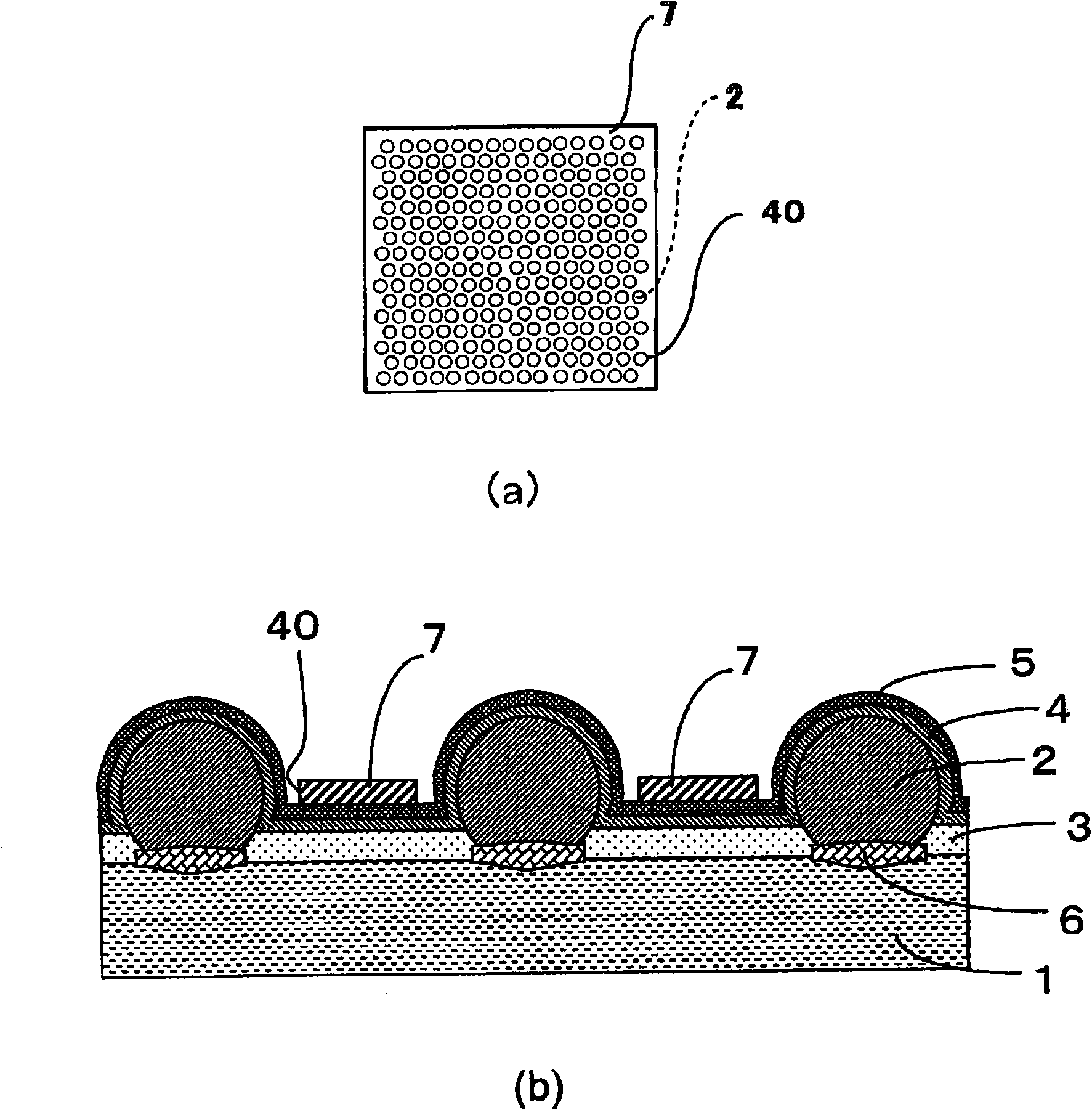
[0053] figure 1 (a) and (b) are a plan view showing an example of the first embodiment of the photoelectric conversion device of the present invention and an enlarged cross-sectional view of main parts thereof, respectively. The photoelectric conversion device of the present invention, such as figure 1 As shown in (b), on the conductive substrate 1, a plurality of spherical crystalline semiconductor particles 2 of the first conductivity type are arranged at intervals from each other, and both are formed by the material of the conductive substrate 1 (for example, aluminum) and crystallization. The material (for example, silicon) of the semiconductor particle 2 is bonded by the cladding layer 6. An insulating layer 3 is formed on the conductive substrate 1 between the crystalline semiconductor particles 2, and a semiconductor layer 4, which is a semiconductor part of the second conductivity type, is formed on the insulating layer 3 and on the crystalline semiconductor particl...

no. 2 Embodiment approach

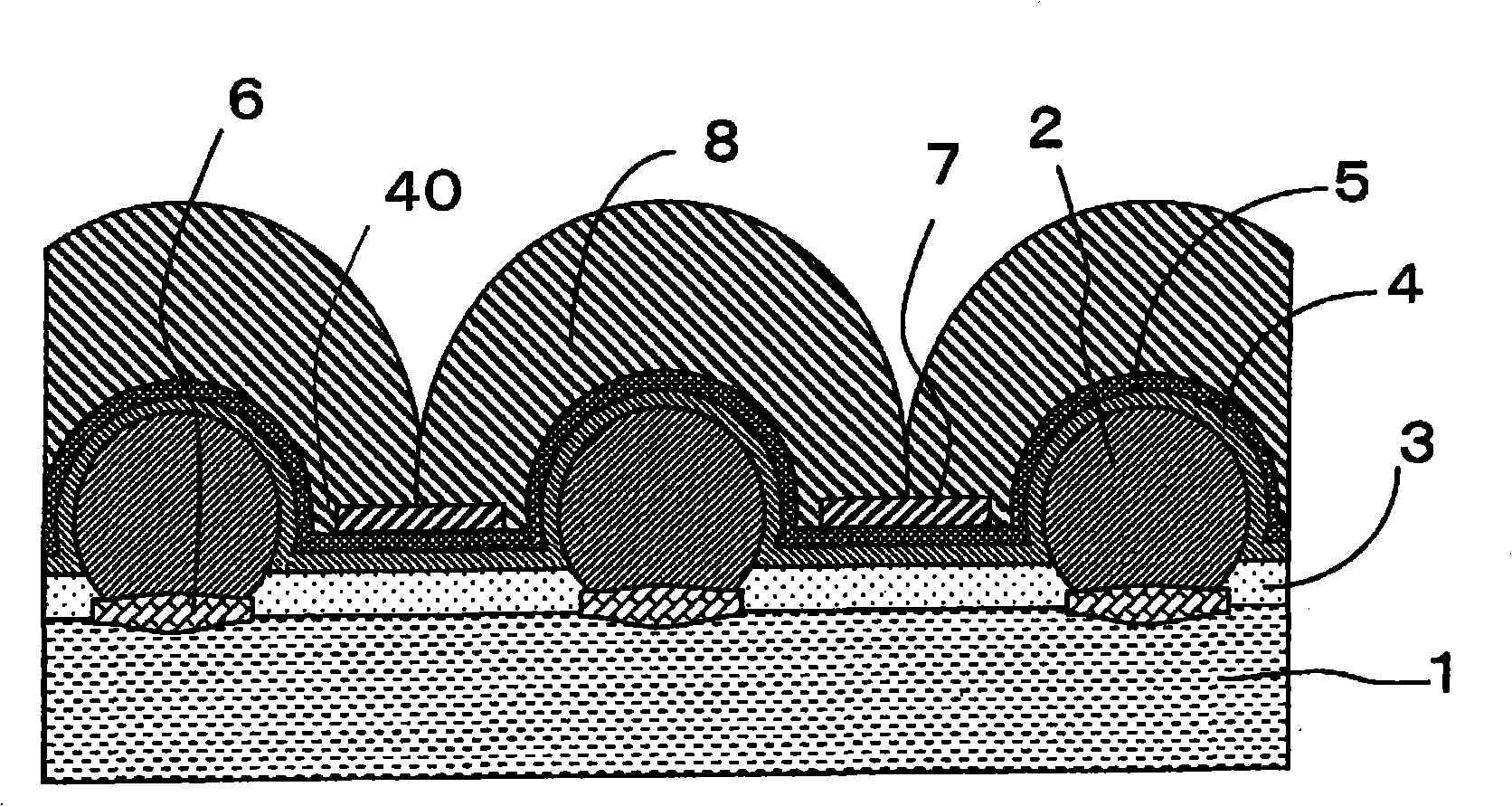
[0083] In the photoelectric conversion device of the first embodiment described above, for example, figure 2 As shown, on the crystalline semiconductor particle 2, a light-transmitting light-collecting layer 8 composed of a lens-shaped member is provided to efficiently introduce light into the crystalline semiconductor particle 2 while avoiding the conductive plate 7 arranged in the non-photoactive part. Light.

[0084] The above-mentioned light-transmitting light-collecting layer 8 is composed of an aspherical shape with a convex curved surface shape on the upper side for the purpose of efficiently taking in light rays at all incident angles into the crystalline semiconductor particles 2, and is formed in each crystalline semiconductor particle. On the translucent conductor layer 5 formed on the particle 2, the outline shape in the longitudinal section is a substantially semicircular convex shape having a diameter larger than that of the crystalline semiconductor particle 2 ...

no. 4 Embodiment approach

[0140] In the present invention, the photoelectric conversion device such as Figure 10 As shown, in the photoelectric conversion device produced in the above-mentioned third embodiment, the translucent light-collecting layer 8 composed of a lens-shaped member capable of efficiently introducing light may be provided on the crystalline semiconductor particles 2 . The translucent light-collecting layer 8 has already been described in the second embodiment.

[0141] According to the above-mentioned structure, by providing the above-mentioned light reflection member 27, even if the area occupied by the crystalline semiconductor particles 2 on the conductive substrate 1 is reduced, the light can be efficiently condensed on the crystalline semiconductor particles 2, and by providing the above-mentioned translucent The light concentrating layer 8 can efficiently introduce light and efficiently condense the light onto the crystalline semiconductor particles 2 . Thereby, while maintai...


PUM


Abstract

A photoelectric conversion device comprises: a plurality of first conduction type crystalline semiconductor grains (2), on each surface layer of which a second conduction type semiconductor portion (4) is formed and which are bonded, at a certain interval, to the surface of a conductive substrate (1); an insulating layer (3) formed between the crystalline semiconductor gains (2) on the conductive substrate (1); a transparent conductive layer (5) formed above the insulating layer (3) and the crystalline semiconductor grains (2); and a collector electrode (7) formed on the surface of the transparent conductive layer (5). The collector electrode (7) consists of a conductive plate having a plurality of through holes (40) that allow external light to illuminate each of the crystalline semiconductor grains (2). Since a transparent light collecting layer (8) is provided on the transparent conductive layer (5) and the collector electrode (7). It is possible to eliminate shadow loss while suppressing resistance loss with a simple process and provide a photoelectric conversion device having a high efficiency.

Description

technical field [0001] The present invention relates to a photoelectric conversion device used for solar power generation, and in particular to an electrode structure and a light-collecting structure in a photoelectric conversion device using crystalline semiconductor particles. Background technique [0002] In general photoelectric conversion devices of the crystalline plate series, an n-type semiconductor region is formed on one main surface side of a p-type silicon substrate to form a pn junction, and a transparent electrode is formed on the entire surface by a light-transmitting conductive layer. A device in which electrodes are respectively formed on the transparent electrode on the one main surface side of the substrate and on the back surface side of the substrate. As the electrodes on the transparent electrode, interdigital electrodes for current collection formed in parallel rows so as not to hinder the incidence of light on the pn junction are generally provided, a...

Claims


Application Information

Patent Timeline
Patent Type & Authority Applications(China)
IPC IPC(8): H01L31/04
CPCY02E10/50
Inventor 冈田健一京田豪林孝一富田贤时有宗久雄
Owner KYOCERA CORP
Why Eureka
Try Eureka