Optical probe for wafer testing

a technology of optical probes and wafers, applied in the field of optical probes for testing optical circuits, can solve the problems of waste of time and effort, fiber mounting, and unable to fully test the device, and the device formed with optical fibers would typically be much larger or not feasible at all

Inactive Publication Date: 2006-03-28
INTEL CORP
View PDF2 Cites 120 Cited by
  • Summary
  • Abstract
  • Description
  • Claims
  • Application Information

AI Technical Summary

Problems solved by technology

Such devices formed with optical fibers would typically be much larger or would not be feasible at all.
However, if the PLC does not

Method used


Image

  • Optical probe for wafer testing
  • Optical probe for wafer testing
  • Optical probe for wafer testing

Examples


Embodiment Construction

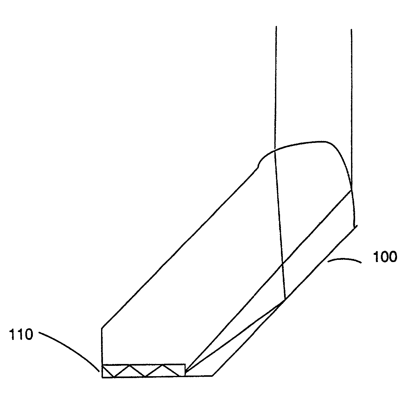
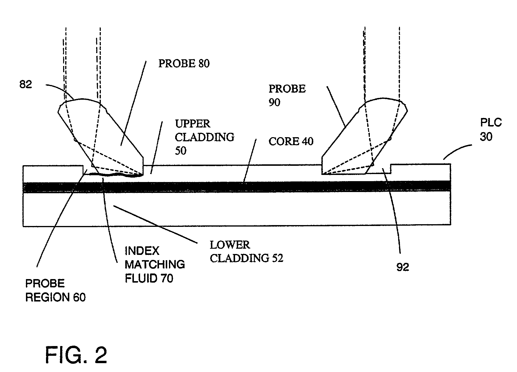
[0012]A method of testing a planar lightwave circuit is achieved by positioning an optical probe in a probe region over a waveguide. In one embodiment, the probe region comprises a waveguide core layer that has either no upper cladding deposited yet, or has a very thin layer of upper cladding deposited. In another embodiment, the probe region has had its upper cladding at least partially removed, e.g., by etching. The remaining upper cladding may be approximately 2 microns or less. In some cases part of the waveguide's core layer may also be removed. A second probe may be used in combination with the first probe to test the planar lightwave circuit by sending and receiving a light beam through the planar lightwave circuit.

[0013]FIG. 2 is a cross-sectional schematic diagram of an optical probe used to test a planar lightwave circuit (PLC) 30. The PLC 30 comprises a waveguide having a core layer 40 and lower cladding 52.

[0014]An optical probe 80 is coupled to the PLC 30 in a probe reg...


PUM


Abstract

A first optical probe is used to test a planar lightwave circuit. In one embodiment, a second probe is used in combination with the first probe to test the planar lightwave circuit by sending and receiving a light beam through the planar lightwave circuit.

Description

BACKGROUND OF THE INVENTION[0001]1. Field of the Invention[0002]The described invention relates to the field of optical circuits. In particular, the invention relates to an optical probe for testing an optical circuit.[0003]2. Description of Related Art[0004]Optical circuits include, but are not limited to, light sources, detectors and / or waveguides that provide such functions as splitting, coupling, combining, multiplexing, demultiplexing, and switching. Planar lightwave circuits (PLCs) are optical circuits that are manufactured and operate in the plane of a wafer. PLC technology is advantageous because it can be used to form many different types of optical devices, such as array waveguide grating (AWG) filters, optical add / drop (de)multiplexers, optical switches, monolithic, as well as hybrid opto-electronic integrated devices. Such devices formed with optical fibers would typically be much larger or would not be feasible at all. Further, PLC structures may be mass produced on a s...

Claims


Application Information

Patent Timeline
IPC IPC(8): G02B6/34G02B6/10G02B6/26G02B6/30G02B6/12G02B6/24G02B6/28
CPCG02B6/12G02B6/34G02B6/30G02B6/2852G02B6/241
Inventor JOHANNESSEN, KJETIL
Owner INTEL CORP
Why Eureka
Try Eureka