Arrangement of microstructures

a microstructure and arrangement technology, applied in the field of semiconductor technology, can solve the problems of increasing the complexity of the structure contained in the integrated circuit, increasing the signal propagation time, and decreasing the limiting frequency, and achieve the effect of reducing the effect of proximity effects

Inactive Publication Date: 2006-04-04
POLARIS INNOVATIONS LTD
View PDF18 Cites 12 Cited by
  • Summary
  • Abstract
  • Description
  • Claims
  • Application Information

AI Technical Summary

Benefits of technology

[0015]Therefore, it is an object of the present invention to specify a method in which the effects of proximity effects are considerably reduced.
[0021]Accordingly, in accordance with the invention, firstly a regular arrangement of closed cavities is formed in a patterning layer. Regular structures can be fabricated with particularly high precision and accuracy in conjunction with a comparatively small extent. On account of the regularity, no local differences occur during the exposure and the etching. Therefore, local proximity effects are avoided particularly during a global regular patterning of the patterning layer. On the other hand, the regularity of the cavities also allows the imaging of cavities which are so small that they can no longer be imaged satisfactorily in the case of separate imaging. The individual cavities are separated from one another by partitions comprising the material of the patterning layer.
[0023]Preferably, the cavities or the depressions etched into the patterning layer in order to form the cavities are defined lithographically and subsequently etched into the pattering layer. In this case, a resist mask may preferably be used for the lithographic definition of the cavities or the depressions, at least two regular strip patterns rotated through a predetermined angle relative to one another being successively imaged into said resist mask. In contrast to raster-shaped patterns, strip patterns can even be imaged with higher accuracy in conjunction with the same resolution. On the other hand, they also enable the imaging of more closely adjacent lines than is possible in the case of a raster-shaped pattern. The possibilities of lithography can be maximally utilized by means of the imaging of strip patterns.
[0038]The method according to the invention also at the same time alleviates the problem of capacitive coupling in particular between interconnects, since, through selection of the cavities to be opened, the interconnects can be placed so that closed cavities remain between adjacent interconnects. Since the dielectric constant εr of said cavities amounts to 1, the dielectric constants taking effect between the adjacent interconnects is correspondingly reduced.
[0044]Cavities between the interconnects make it possible to reduce the capacitive couplings between the interconnects and thus generally capacitive couplings and signal delays.
[0045]It is possible to have recourse to all the advantages of the damascene method, e.g. patterning of materials that cannot be etched or are difficult to etch.

Problems solved by technology

Advancing scaling of integrated circuits and the associated miniaturization and increasing complexity of the structures contained in the integrated circuits entail a multiplicity of problems.
Associated with this is an unfavorable rise in the RC time constants, which lead to rising signal propagation times, decreasing limiting frequencies, high power loss densities and crosstalk effects.
In the fabrication of integrated circuits, these effects lead to structural results which deviate from the desired structures prescribed on the lithography mask.
Diverse organic dielectrics having dielectric constants of approximately 2:5 are used as “low-k dielectrics” (e.g. so-called aerogels or xerogels, U.S. Pat. No. 6,277,728, whose disclosure is incorporated herein by reference thereto), but they are usually associated with diverse disadvantages (low thermal and chemical stability, hygroscopy, low blocking effect against the diffusion of e.g. copper, need to develop new deposition and patterning processes, new process installations).
Porous inorganic dielectrics having even lower dielectric constants (e.g. porous SiON) are not yet ready for production at the present time.
The above-mentioned methods have the disadvantage of a relatively high process complexity.
However, the fundamental problems going back to the proximity effects of lithography and etching technology are not avoided with the abovementioned methods.

Method used


Image

  • Arrangement of microstructures
  • Arrangement of microstructures
  • Arrangement of microstructures

Examples


Embodiment Construction

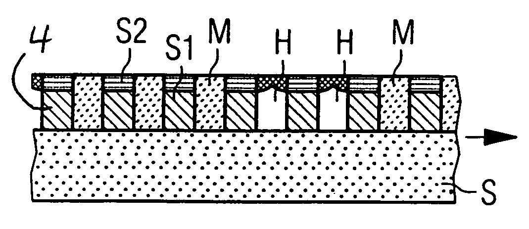
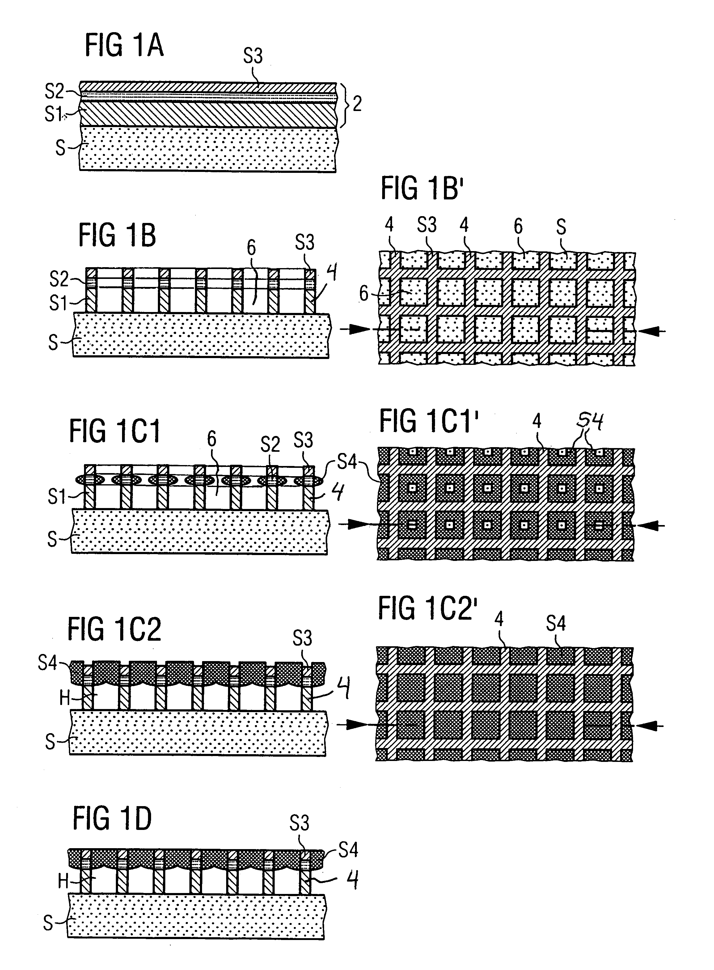
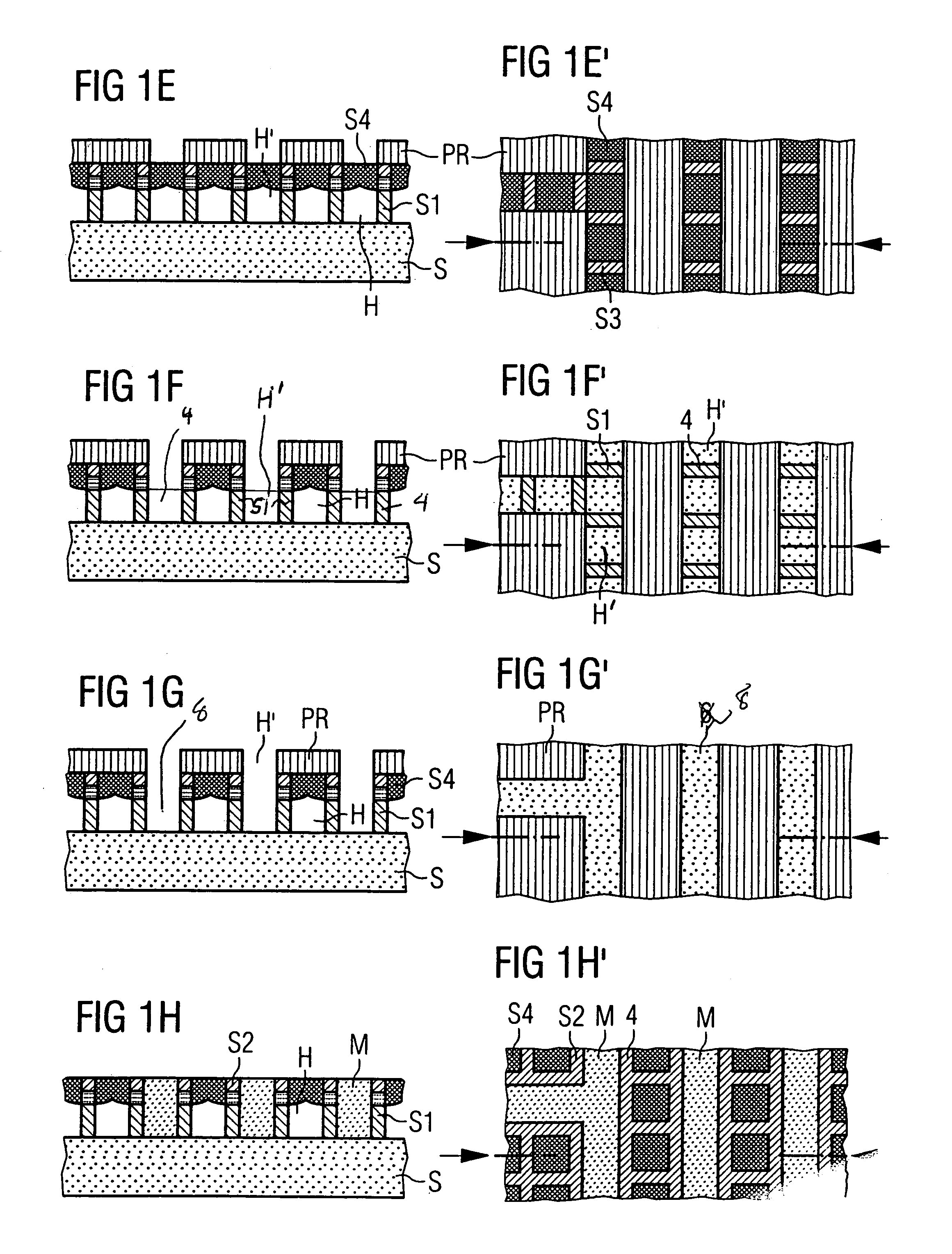
[0060]FIGS. 1A–1I′ show an embodiment of the “cellular damascene method”, in which the microstructures to be fabricated are separated from one another by cavities. The cavity pattern produced in this case extends over the entire surface of a chip to be fabricated or at least over the majority of its area.

[0061]FIG. 1A is a cross-sectional view that shows a substrate S, on which three dielectric layers S1, S2 and S3 have been successively deposited. At least the material of the second layer S2 differs from the material of the first layer S1 and of the third layer S3. By way of example, the first and third layers S1 and S3 may comprise silicon nitride and the second layer S2 may comprise silicon oxide which has been formed by means of a plasma-enhanced deposition from a silane atmosphere. In this case, the first layer S1 performs the function of a carrier layer and defines the height of the cavities that are subsequently to be formed. For this reason, this layer has a thickness that i...


PUM

PropertyMeasurementUnit
angleaaaaaaaaaa
dielectric constantsaaaaaaaaaa
sharp anglesaaaaaaaaaa

Abstract

A method referred to as a “cellular damascene method” utilizes a multiplicity of regularly arranged closed cavities referred to as “cells”, which are produced in a patterning layer. The dimensions of the cavities are on the order of magnitude of the microstructures to be produced. Selected cavities are opened by providing a mask and partitions situated between adjacent opened cavities are removed to provide trenches and holes which are filled with the material of the microstructure to be fabricated. Protruding material is removed by means of a chemical-mechanical polishing step. The microstructures are, in particular, interconnects and contact holes of integrated circuit.

Description

CROSS-REFERENCE TO RELATED APPLICATION[0001]This application is a divisional of U.S. Ser. No. 10 / 606,069, filed Jun. 25, 2003, which issued as U.S. Pat. No. 6,825,098.BACKGROUND OF THE INVENTION[0002]The invention is in the field of semiconductor technology and relates to a method for fabricating microstructures.[0003]Advancing scaling of integrated circuits and the associated miniaturization and increasing complexity of the structures contained in the integrated circuits entail a multiplicity of problems.[0004]Thus, by way of example, the interconnect resistances of the individual interconnects within the wiring planes increase. The capacitive coupling between the interconnects increases at the same time. Associated with this is an unfavorable rise in the RC time constants, which lead to rising signal propagation times, decreasing limiting frequencies, high power loss densities and crosstalk effects. The technical literature also groups these problems under the term “wiring crisis”...

Claims


Application Information

Patent Timeline
Patent Type & Authority Patents(United States)
IPC IPC(8): H01L31/113H01L21/768H01L23/522
CPCH01L21/7682H01L23/5222H01L2924/0002H01L2924/00
Inventor GABRIC, ZVONIMIRPAMLER, WERNERSCHWARZL, SIEGFRIED
Owner POLARIS INNOVATIONS LTD
Why Eureka
Try Eureka