

Method for improving design window
a technology of design window and via, applied in the field of semiconductor integrated circuit fabrication process, can solve the problems of affecting the performance and reliability of the fabricated circuit, both reliability and performance problems in the integrated circuit, self-heating effects, etc., and achieves the effect of reducing optical proximity effects and increasing spacing between vias
- Summary
- Abstract
- Description
- Claims
- Application Information
AI Technical Summary
Benefits of technology
Problems solved by technology
Method used
Image

Examples
Embodiment Construction
[0024] The making and using of the presently preferred embodiments are discussed in detail below. It should be appreciated, however, that the present invention provides many applicable inventive concepts that can be embodied in a wide variety of specific contexts. The specific embodiments discussed are merely illustrative of specific ways to make and use the invention, and do not limit the scope of the invention.
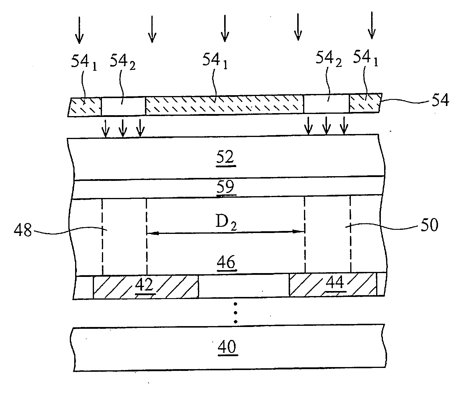
[0025] A novel method for forming photo masks and for forming vertical conductive features is illustrated. The variations of the preferred embodiments are discussed. Throughout the various views and illustrative embodiments of the present invention, like reference numbers are used to designate like elements. For simplicity purposes, the subsequently discussions focus on vias and their formation method. However, the same concepts equally apply to other vertical conductive features, such as contacts. By improving spacing between vertical conductive features, design windows ar...
PUM
| Property | Measurement | Unit |
|---|---|---|
| dielectric constant | aaaaa | aaaaa |
| wavelength | aaaaa | aaaaa |
| wavelengths | aaaaa | aaaaa |
Abstract
Description
Claims
Application Information