Method and system for implementing edge optimization on an integrated circuit design

a technology of integrated circuits and optimization methods, applied in error detection/correction, total factory control, instruments, etc., can solve the problems of reducing the accuracy of requiring extreme precision for sub wavelengths or low-kl, and increasing the challenge of manufacturing modern ic designs using conventional optical lithography technology, etc., to achieve the effect of reducing the distortion of optical proximity effect, and reducing the number of mask errors

Active Publication Date: 2010-05-18
CADENCE DESIGN SYST INC
View PDF28 Cites 8 Cited by
  • Summary
  • Abstract
  • Description
  • Claims
  • Application Information

AI Technical Summary

Benefits of technology

[0007]The manufacturability of modern IC designs using conventional optical lithography technology is increasingly being challenged by the sub wavelength, or low-kl, dimensions of the critical. IC feature geometries. Not only are the critical dimension feature geometries decreasing in size in accordance with, or even faster than, Moore's Law predictions, the already large number of these feature geometries is growing at a dramatic rate as well. Furthermore, due to the necessity to mitigate optical proximity effect distortions through resolution enhancement techniques at the mask level, the overall polygonal figure count is skyrocketing. These critical feature geometries are patterned far more precisely as well due to the severity and sensitivity of the non-linear imaging. Extreme precision is required for sub wavelength, or low-kl, applications due to highly non-linear imaging behaviors which often magnify mask errors by large factors and non-intuitive manners.

Problems solved by technology

The manufacturability of modern IC designs using conventional optical lithography technology is increasingly being challenged by the sub wavelength, or low-kl, dimensions of the critical.
Furthermore, due to the necessity to mitigate optical proximity effect distortions through resolution enhancement techniques at the mask level, the overall polygonal figure count is skyrocketing.
Extreme precision is required for sub wavelength, or low-kl, applications due to highly non-linear imaging behaviors which often magnify mask errors by large factors and non-intuitive manners.
In deep submicron design, a significant amount of time and effort is usually spent dealing with design manufacturability rules.
The problem is that conventional approaches for handling design rules tend to break down when handling deep submicron designs.

Method used


Image

  • Method and system for implementing edge optimization on an integrated circuit design
  • Method and system for implementing edge optimization on an integrated circuit design
  • Method and system for implementing edge optimization on an integrated circuit design

Examples


Embodiment Construction

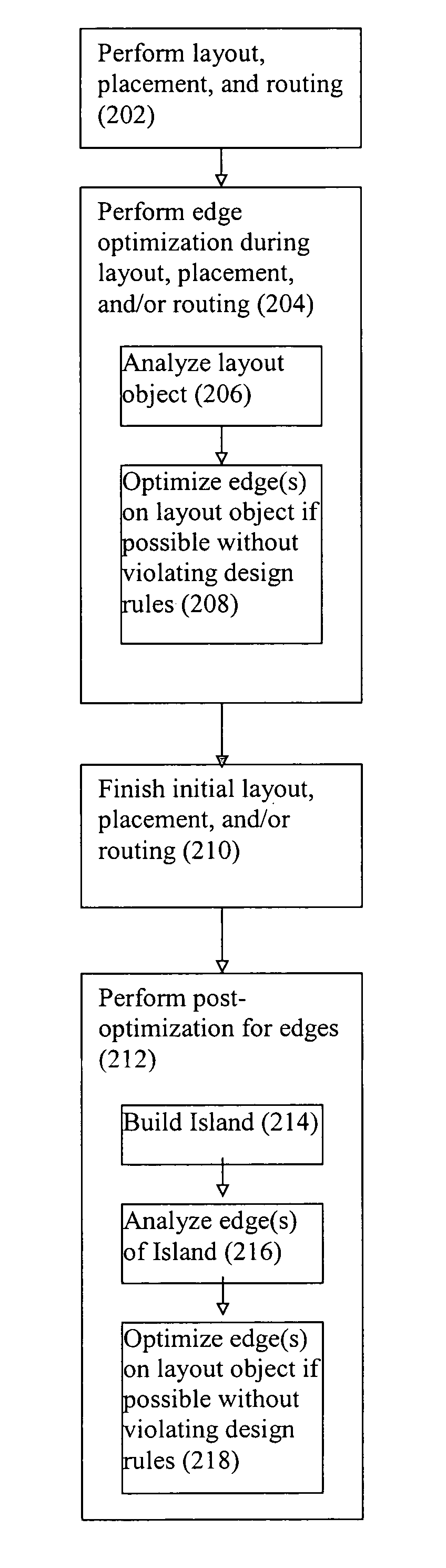
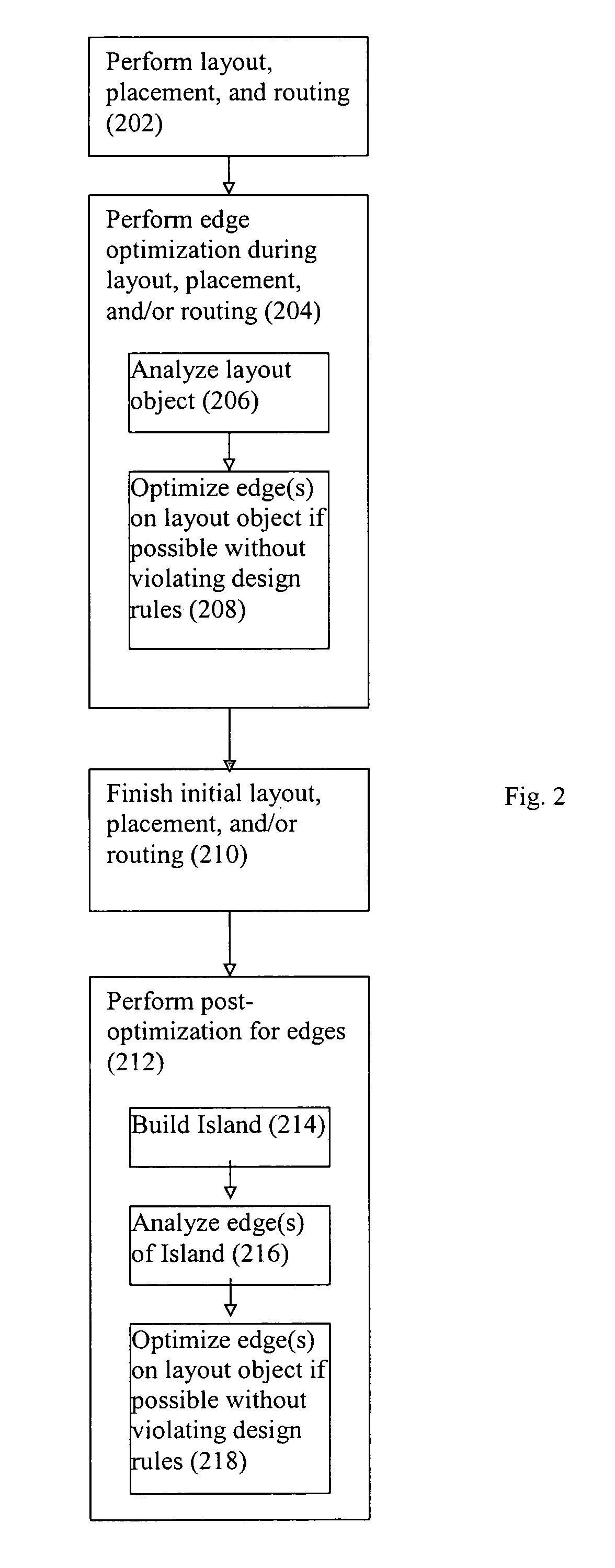
[0014]Conventional electronic design tools do not specifically focus on edge characteristics and optimization when placing and routing layout objects. However, conventional approaches for handling electronic designs and design rules tend to break down when handling deep submicron designs. In particular, with smaller designs such as 65 nanometer designs, 45 nanometer designs, or even smaller designs, the edge characteristics of layout objects may critically affect the manufacturability, reliability, and operability of integrated circuits.

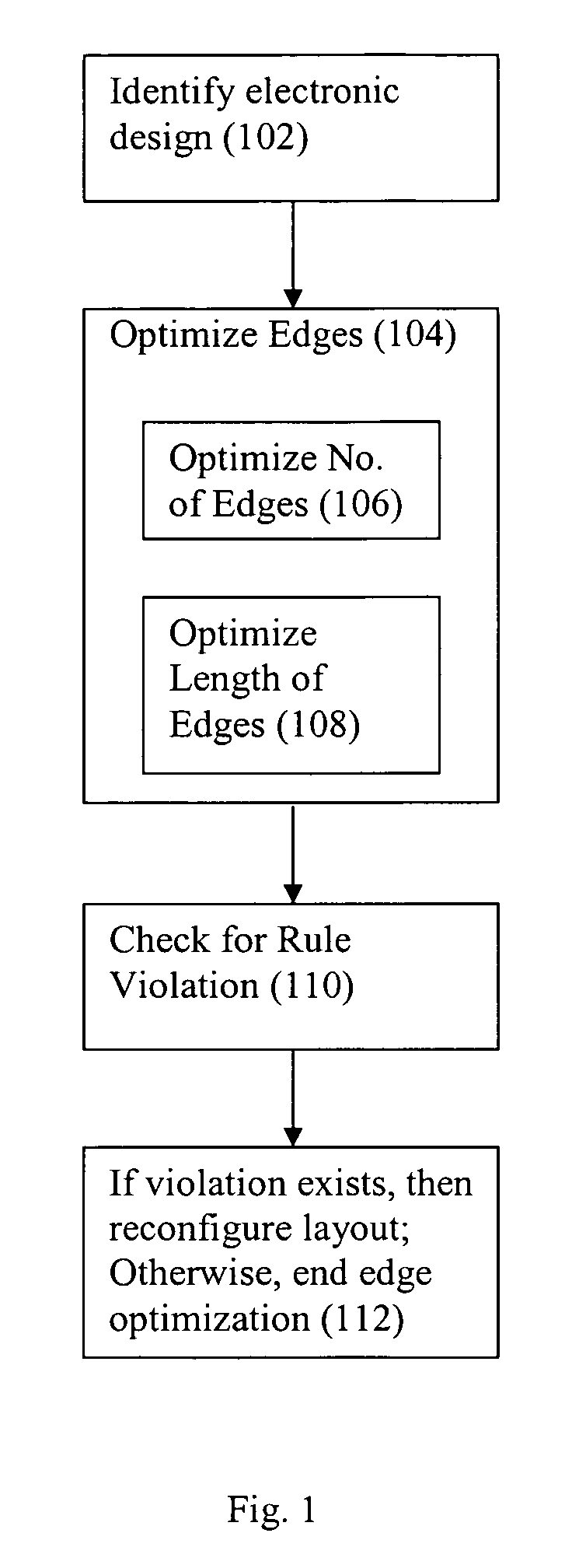
[0015]The present invention is directed to a method, system, and computer program product for performing edge optimization on an electronic design. FIG. 1 shows a flowchart of a process for performing edge optimization according to some embodiments of the invention. The process begins by identifying an electronic design to be optimized (102).

[0016]The layout objects are analyzed and adjusted to optimize the objects' edge characteristics (104). In som...


PUM


Abstract

Disclosed is a method, system, and computer program product for performing edge optimization on an electronic design. According to some approaches, the number of edges and/or the length of edges within an IC design are configured for optimized manufacturability and yield of an integrated circuit. The edge optimization may occur in real-time during layout, placement, and/or routing, or occur in a post-optimization step.

Description

CROSS-REFERENCE TO RELATED APPLICATIONS[0001]The present application claims the benefit of U.S. Provisional Application No. 60 / 817,622, filed on Jun. 28, 2006, which is hereby incorporated by reference in its entirety.BACKGROUND AND SUMMARY[0002]A semiconductor integrated circuit (IC) has a large number of electronic components, such as transistors, logic gates, diodes, wires, etc., that are fabricated by forming layers of different materials and of different geometric shapes on various regions of a silicon wafer.[0003]Many phases of physical design may be performed with computer aided design (CAD) tools or electronic design automation (EDA) systems. To design an integrated circuit, a designer first creates high level behavior descriptions of the IC device using a high-level hardware design language. An EDA system typically receives the high level behavior descriptions of the IC device and translates this high-level design language into netlists of various levels of abstraction usin...

Claims


Application Information

Patent Timeline
Patent Type & Authority Patents(United States)
IPC IPC(8): G06F17/50
CPCG06F17/5072G06F17/5081G06F17/5077G06F2217/12G06F30/398G06F2119/18G06F30/392G06F30/394Y02P90/02
Inventor NEQUIST, ERICBRASHEARS, RICHARD
Owner CADENCE DESIGN SYST INC
Why Eureka
Try Eureka