Method and system for implementing layout, placement, and routing with merged shapes

a technology of layout and placement, applied in error detection/correction, total factory control, instruments, etc., can solve the problems of reducing the accuracy of increasing the difficulty of manufacturing modern ic designs using conventional optical lithography technology, and requiring extreme precision for sub wavelengths. , to achieve the effect of reducing the distortion of optical proximity effect, reducing the difficulty of manufacturing, and reducing the cost of production

Inactive Publication Date: 2009-09-15
CADENCE DESIGN SYST INC
View PDF2 Cites 7 Cited by
  • Summary
  • Abstract
  • Description
  • Claims
  • Application Information

AI Technical Summary

Benefits of technology

[0007]The manufacturability of modern IC designs using conventional optical lithography technology is increasingly being challenged by the sub wavelength, or low-k1, dimensions of the critical IC feature geometries. Not only are the critical dimension feature geometries decreasing in size in accordance with, or even faster than, Moore's Law predictions, the already large number of these feature geometries is growing at a dramatic rate as well. Furthermore, due to the necessity to mitigate optical proximity effect distortions through resolution enhancement techniques at the mask level, the overall polygonal figure count is skyrocketing. These critical feature geometries are patterned far more precisely as well due to the severity and sensitivity of the non-linear imaging. Extreme precision is required for sub wavelength, or low-k1, applications due to highly non-linear imaging behaviors which often magnify mask errors by large factors and non-intuitive manners.

Problems solved by technology

The manufacturability of modern IC designs using conventional optical lithography technology is increasingly being challenged by the sub wavelength, or low-k1, dimensions of the critical IC feature geometries.
Furthermore, due to the necessity to mitigate optical proximity effect distortions through resolution enhancement techniques at the mask level, the overall polygonal figure count is skyrocketing.
Extreme precision is required for sub wavelength, or low-k1, applications due to highly non-linear imaging behaviors which often magnify mask errors by large factors and non-intuitive manners.
In deep submicron design, a significant amount of time and effort is usually spent dealing with design manufacturability rules.
The problem is that conventional approaches for handling design rules tend to break down when handling deep submicron designs.

Method used


Image

  • Method and system for implementing layout, placement, and routing with merged shapes
  • Method and system for implementing layout, placement, and routing with merged shapes
  • Method and system for implementing layout, placement, and routing with merged shapes

Examples


Embodiment Construction

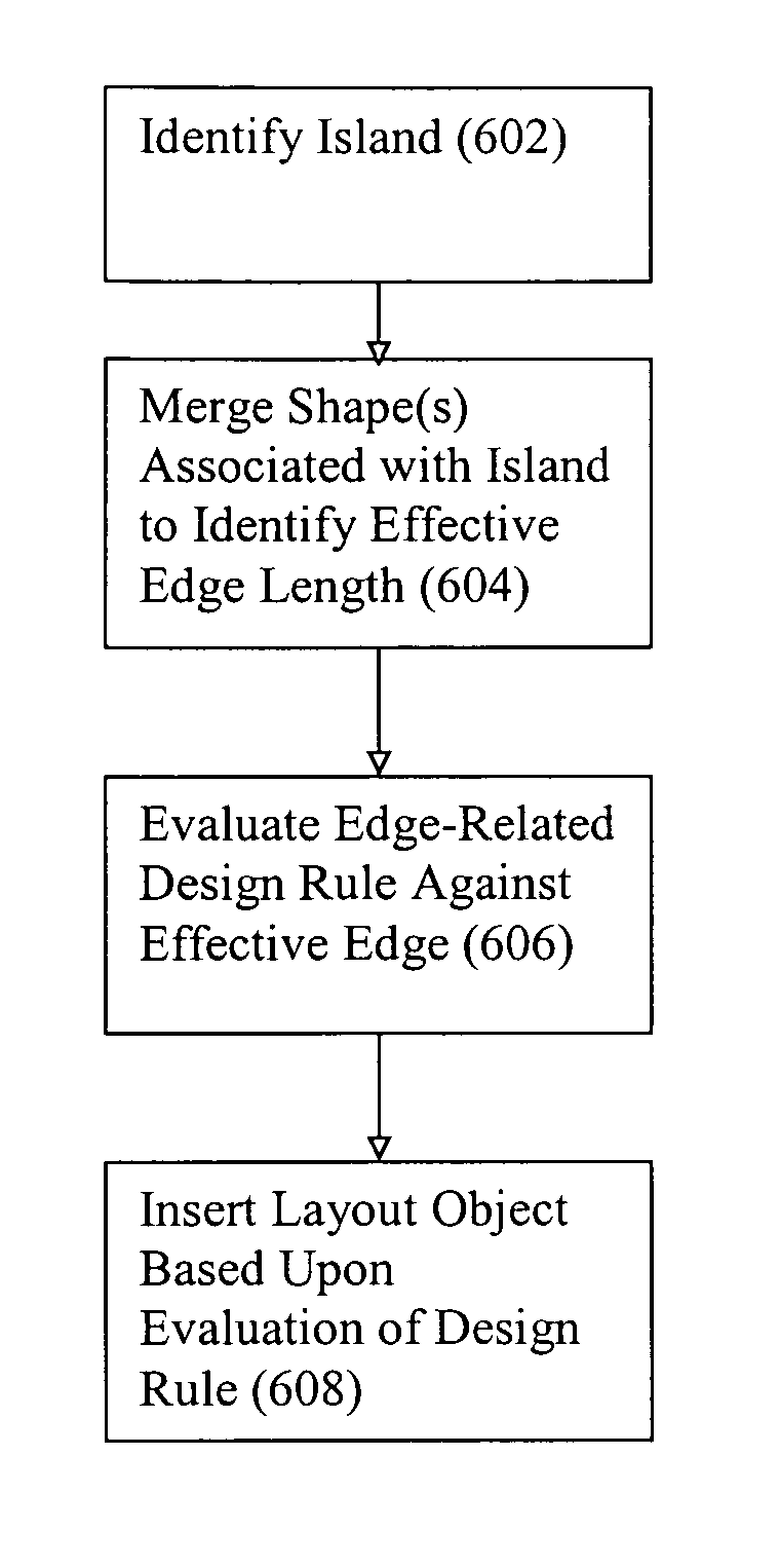
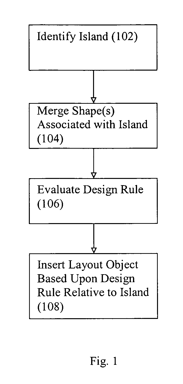
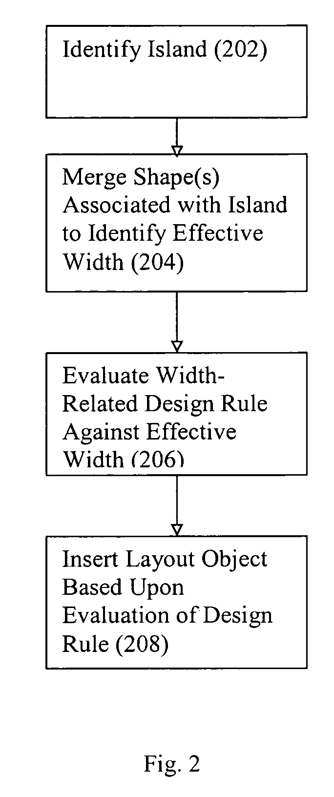
[0019]The present invention is directed to an improved method, system, and computer program product for performing layout, placement, and / or routing for electronic designs. As noted above, conventional systems separately and individually consider existing objects in the layout when determining the appropriate location and / or configuration of polygons to place or route in the design.

[0020]According to some embodiments of the invention, multiple objects, or even relevant portions of those objects, are considered together as a collective object or shape. The collective object or shape is then considered when analyzing design rules for placement of other objects in the layout.

[0021]FIG. 1 shows a high level flowchart of a process for performing layout, placement, and / or routing according to an embodiment of the invention. One or more “islands” are formed based upon the proximity of one or more of the objects relative to one or more other objects (102). An island refers to a set of objec...


PUM


Abstract

Disclosed is an improved method, system, and computer program product for performing layout, placement, and routing for electronic designs. According to some approaches, multiple objects are considered as a collective object or shape, based upon the proximity of one or more of the objects to one or more other objects. The type and/or configuration of the collective object is based, for example, upon the type of rule that is being considered for the layout, placement, or routing operation.

Description

CROSS-REFERENCE TO RELATED APPLICATIONS[0001]The present application claims the benefit of U.S. Provisional Application No. 60 / 817,602, filed on Jun. 28, 2006, which is hereby incorporated by reference in its entirety.BACKGROUND AND SUMMARY[0002]A semiconductor integrated circuit (IC) has a large number of electronic components, such as transistors, logic gates, diodes, wires, etc., that are fabricated by forming layers of different materials and of different geometric shapes on various regions of a silicon wafer.[0003]Many phases of physical design may be performed with computer aided design (CAD) tools or electronic design automation (EDA) systems. To design an integrated circuit, a designer first creates high level behavior descriptions of the IC device using a high-level hardware design language. An EDA system typically receives the high level behavior descriptions of the IC device and translates this high-level design language into netlists of various levels of abstraction usin...

Claims


Application Information

Patent Timeline
Patent Type & Authority Patents(United States)
IPC IPC(8): G06F17/50
CPCG06F17/5081G06F2217/12G06F30/398G06F2119/18Y02P90/02
Inventor NEQUIST, ERICBRASHEARS, RICHARD
Owner CADENCE DESIGN SYST INC
Why Eureka
Try Eureka