Optical device having dual microstrip transmission lines with a low-k material and a method of manufacture thereof

a transmission line and optical device technology, applied in the field of optical devices, can solve the problems of 40 ghz, difficult to achieve a wide operation bandwidth, and practically impossible to achieve the desired wide bandwidth operation mentioned above with a lumped-element electrod

Inactive Publication Date: 2006-04-04
QORVO US INC
View PDF6 Cites 19 Cited by
  • Summary
  • Abstract
  • Description
  • Claims
  • Application Information

AI Technical Summary

Benefits of technology

[0010]To address the above-discussed deficiencies of the prior art, the present invention provides an optical device. In one embodiment, the optical device includes an optical waveguide formed on a ridge located on a substrate. The optical device also includes a microstrip transmission line ...

Problems solved by technology

Due to this fact, the required modulation length for achieving low modulation voltage (Vn<5V) makes it difficult to achieve a wide operational bandwidth (e.g., 30–40 GHz).
However, such a relatively long modulation waveguide usually contains a large modulation loading capacitance (CL˜4 pF), which makes it practically impossible to achieve the desired wide bandwidth operation mentioned above with a lumped-element electrode.
Unfortunately, a typical III–V MZM using the push-pull scheme with traveling-wave electrodes still cannot safely meet the system requirement.
From these results, those who are skilled in the art understand that the operational bandwidth for the traveling-wave MZM is thus limited by the ...

Method used


Image

  • Optical device having dual microstrip transmission lines with a low-k material and a method of manufacture thereof
  • Optical device having dual microstrip transmission lines with a low-k material and a method of manufacture thereof
  • Optical device having dual microstrip transmission lines with a low-k material and a method of manufacture thereof

Examples


Embodiment Construction

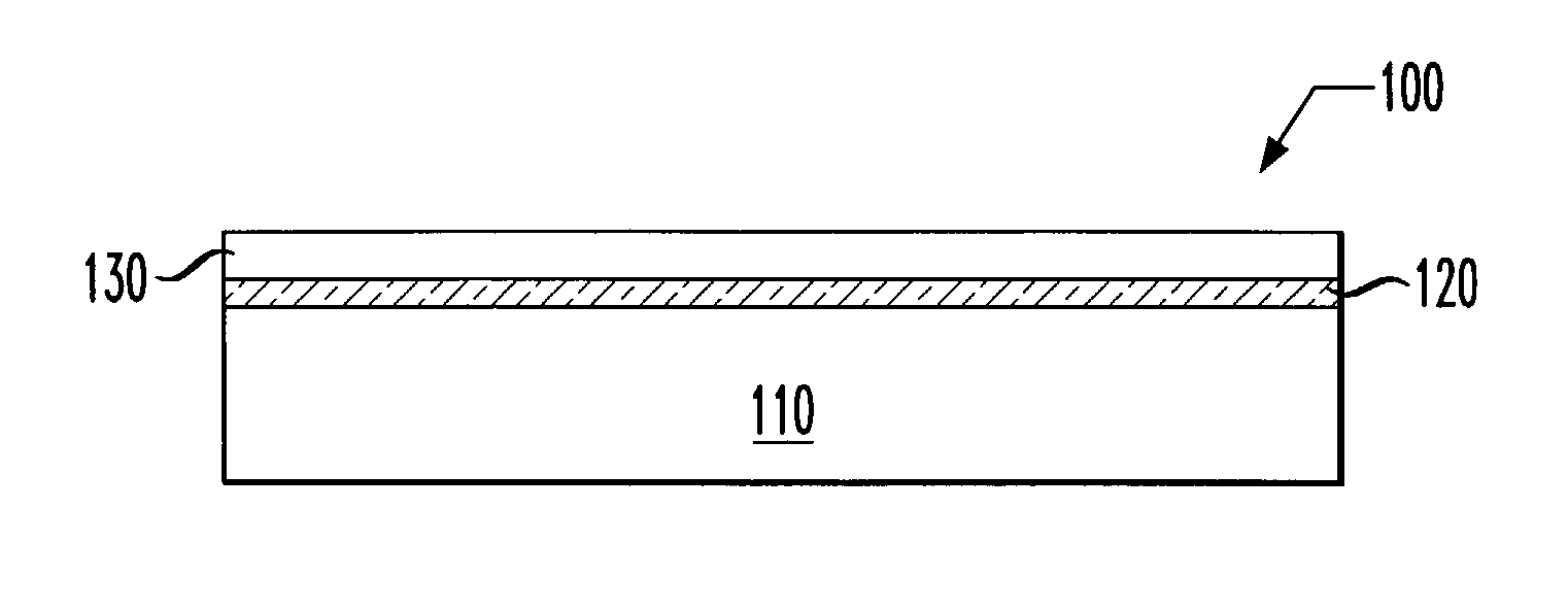
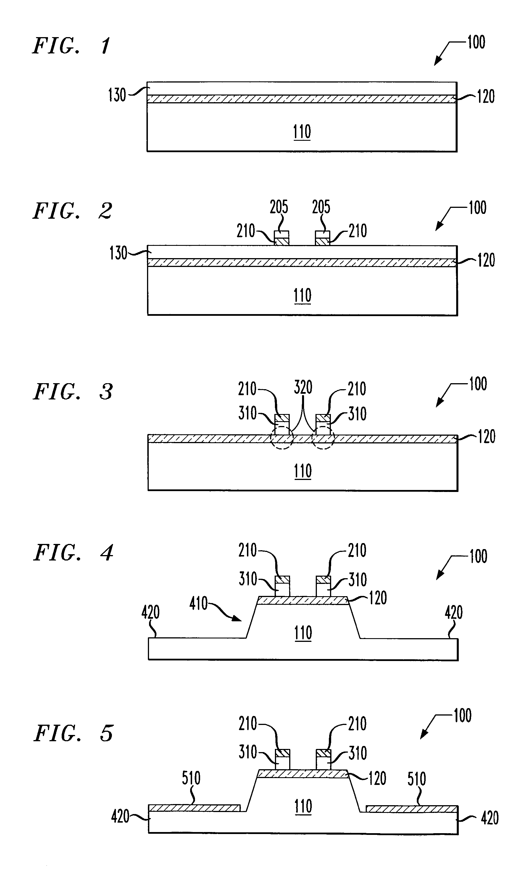
[0027]Referring initially to FIG. 1, illustrated is one embodiment of an initial device 100 early in a manufacturing process according to the principles of the present invention. The initial device 100 includes a semiconductor substrate 110, which in an exemplary embodiment, may be an N+ substrate 110 having a high dielectric constant (k). In a more specific embodiment, the substrate 110 may be an indium phosphate (InP) substrate 110, however other appropriate semiconductor materials, such as gallium arsenide (GaAs), may be employed.

[0028]Formed over the substrate 110 is an active modulation layer 120. The active modulation layer 120 may comprise, for example, indium / gallium / arsenide / phosphate (InGaAsP) bulk layers or InGaAsP / InP multiple quantum wells. However, other materials such as indium / gallium / aluminum / arsenide (InGaAlAs) bulk layers or InGaAlAs / InAlAs multiple quantum wells may also be used on an InP substrate. GaAs may be used as the active modulation layer 120 on a GaAs su...


PUM


Abstract

The present invention provides an optical device. In one embodiment, the optical device includes an optical waveguide formed in or over a ridge located on a substrate. The optical device also includes a microstrip transmission line comprising a signal electrode and a ground electrode adjacent the ridge and a low-k dielectric material separating the signal and ground electrodes. The present invention also provides a method for making the optical device.

Description

TECHNICAL FIELD OF THE INVENTION[0001]The present invention is directed, in general, to optical devices and, more specifically, to an optical device having an optical waveguide formed over or in a ridge, a microstrip transmission line comprising a signal electrode and a ground electrode adjacent the ridge, and a low-k dielectric material separating the signal and ground electrodes.BACKGROUND OF THE INVENTION[0002]Optical communication systems have continued to gain popularity in today's data transmission markets. Primarily because of their fast transmission speed, small size and relatively precise manufacture, Optical communication systems incorporating numerous optical devices and assemblies have become the systems of choice for technology companies desiring high-speed information transmission capabilities. Accordingly, as the transfer of information becomes one of the most valuable commodities in the world, optical device manufacturers are eager to develop further improvements in ...

Claims


Application Information

Patent Timeline
IPC IPC(8): G02F1/01G02F1/035G02F1/017
CPCB82Y20/00G02F1/225G02F1/01708G02F2201/122
Inventor LI, GUOLIANGMASON, THOMAS G. B.
Owner QORVO US INC
Why Eureka
Try Eureka