Magnetic shift register with shiftable magnetic domains between two regions, and method of using the same

a magnetic domain and magnetic shift register technology, applied in the field of memory storage systems, can solve the problems of solid-state random access memories, devices with moving parts tend to wear out and fail, and the magnetic shift register can be varied, and achieve the effect of high cost of mechanical means, high reading cost, and high cost of magnetic shift registers

Inactive Publication Date: 2006-04-18
GLOBALFOUNDRIES U S INC
View PDF2 Cites 126 Cited by
  • Summary
  • Abstract
  • Description
  • Claims
  • Application Information

AI Technical Summary

Benefits of technology

[0016]An important characteristic of domain wall fringing fields is that they are localized in small regions of space near the domain wall. Thus, domain wall fringing fields can provide highly localized and large magnetic fields that can be manipulated in space by moving or controlling the position of the domain wall within a magnetic entity such as a magnetic wire. Since the magnitude of the fringing fields drops rapidly with distance from the domain wall, application of the domain wall fringing fields can be controlled in wires by varying the distance of the wire from the material, whose property is to be changed by the domain wall fringing field and by moving the domain wall along the wire.
[0022]The magnetic shift register described herein, presents numerous advantages over other forms of solid state memory and magnetic recording hard disk drives. In particular, the magnetic shift register provides a means of accessing hundreds of data bits using a small number of logic gates and circuit elements. Thus, the magnetic shift register can provide capacious amounts of storage comparable to those provided in conventional hard disk drives but without any moving parts and at a comparable cost of such hard disk drives.
[0023]Similarly, compared to conventional solid state memory devices, the magnetic shift register provides far higher memory capacities but at a fraction of the cost per bit of conventional solid state memories. This advantage is achieved because the magnetic shift register can be fabricated using standard CMOS processes and methods of manufacture but the magnetic shift register stores hundreds of data bits for the same area of silicon in which a conventional CMOS solid state memory would store one or a small number of bits.
[0024]This latter advantage is realized because the magnetic shift register uses the third dimension out of the plane of the silicon substrate to store data in largely vertical tracks which occupy little space on the silicon substrate. Since the cost of CMOS logic and memory is largely determined by the area of silicon used in any given technology node the magnetic shift register can thereby provide a far cheaper means of storing data than conventional solid state memories.
[0026]The capacity of the magnetic shift register can be varied over a wide range continuously by simply varying the number of magnetic shift register tracks per memory device. This is a particular advantage over magnetic hard disk drives in which because of the high cost of the reading and writing heads and their circuitry, and the high cost of the mechanical means of moving these heads and the magnetic media, a hard disk drive only provides a cheap means of storage when many gigabytes of data are stored, such that the cost of the mechanical components of the hard disk drive is amortized over the large number of data bits.
[0027]By contrast, the magnetic shift register can be built at low cost per bit in much smaller sizes, thereby allowing the magnetic shift register to be used for a wide range of applications where the data storage capacity required is much lower than that of a magnetic hard disk drive. Thus the magnetic shift register can be used for various electronic devices including by way of example, but not limited to: digital cameras, personal digital assistants, security devices, memory sticks, removable storage devices, and so forth.

Problems solved by technology

However, disk drives are inherently unreliable.
Devices with moving parts tend to wear out and fail.
Solid state random access memories currently store data on the order of 1 GB (gigabyte) per device, and are relatively expensive, per storage unit, i.e., per 1 GB, compared to a disk drive.
In addition, flash memory cells could begin to lose data after less than a million write cycles.
While this may be adequate for some applications, flash memory cells would begin to fail rapidly if used constantly to write new data, such as in a computer's main memory.
Further, the access time for flash memory is much too long for computer applications.
However, commercially available memory capacities are currently low, on the order of 0.25 MB (megabyte).
In addition, memory storage in a FRAM relies on physically moving atoms, leading to eventual degradation of the medium and failure of the memory.
However, the size of these memories is still small, on the order of 4 MB currently.
In addition, OUM relies on physically changing a material from crystalline to amorphous; which likely causes the material to eventually degrade and fail.
However, currently available MRAM can only store up to 1 Mb (megabit), much less than needed for most memory applications.
In addition, each MRAM memory cell stores only one bit of data, thereby limiting the maximum possible memory capacity of such devices.
The need for such a system has heretofore remained unsatisfied.

Method used


Image

  • Magnetic shift register with shiftable magnetic domains between two regions, and method of using the same
  • Magnetic shift register with shiftable magnetic domains between two regions, and method of using the same
  • Magnetic shift register with shiftable magnetic domains between two regions, and method of using the same

Examples


Embodiment Construction

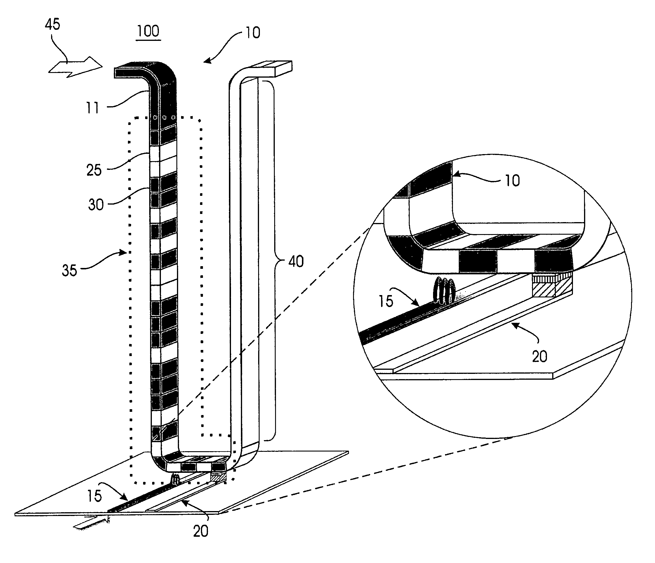
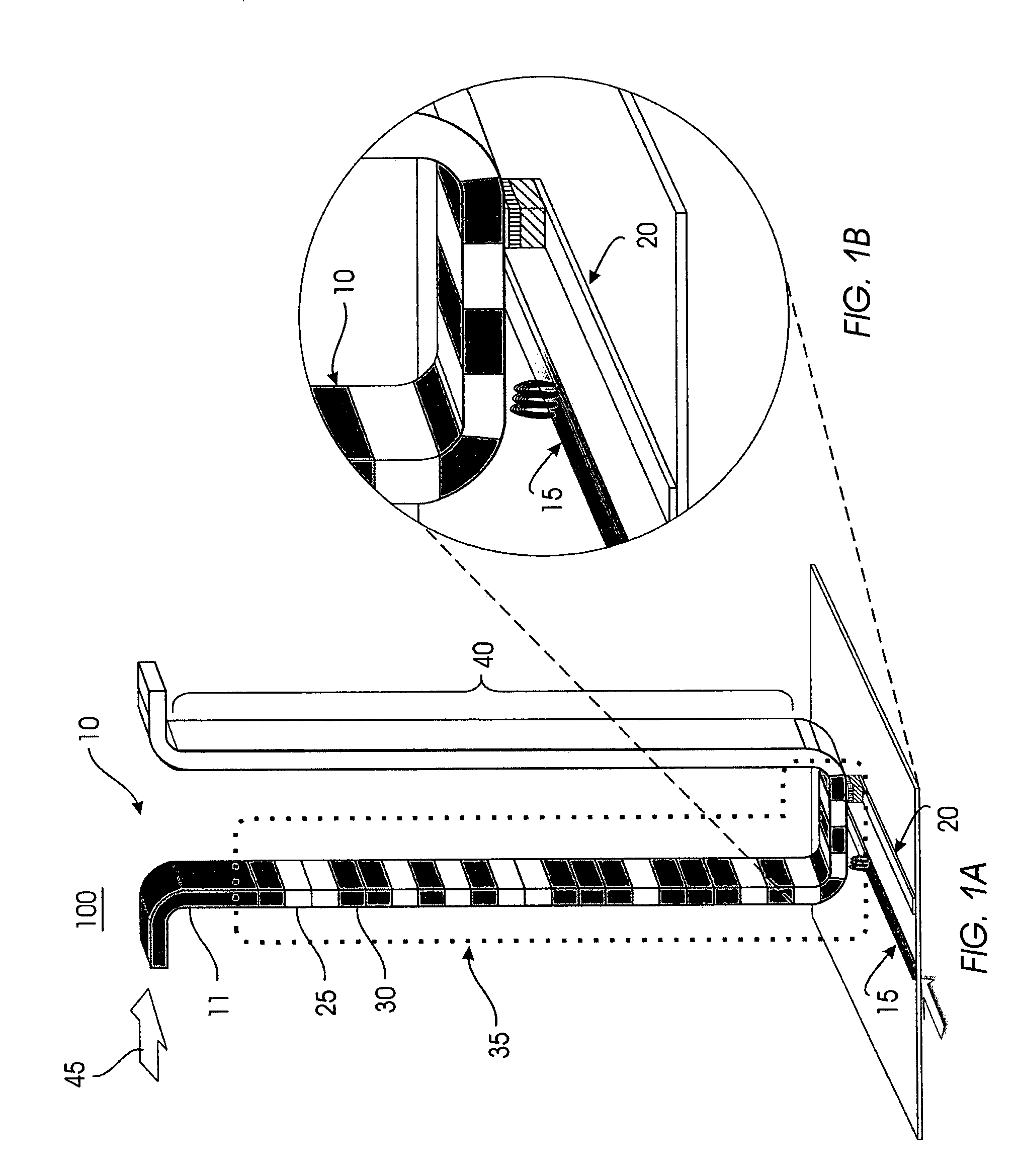
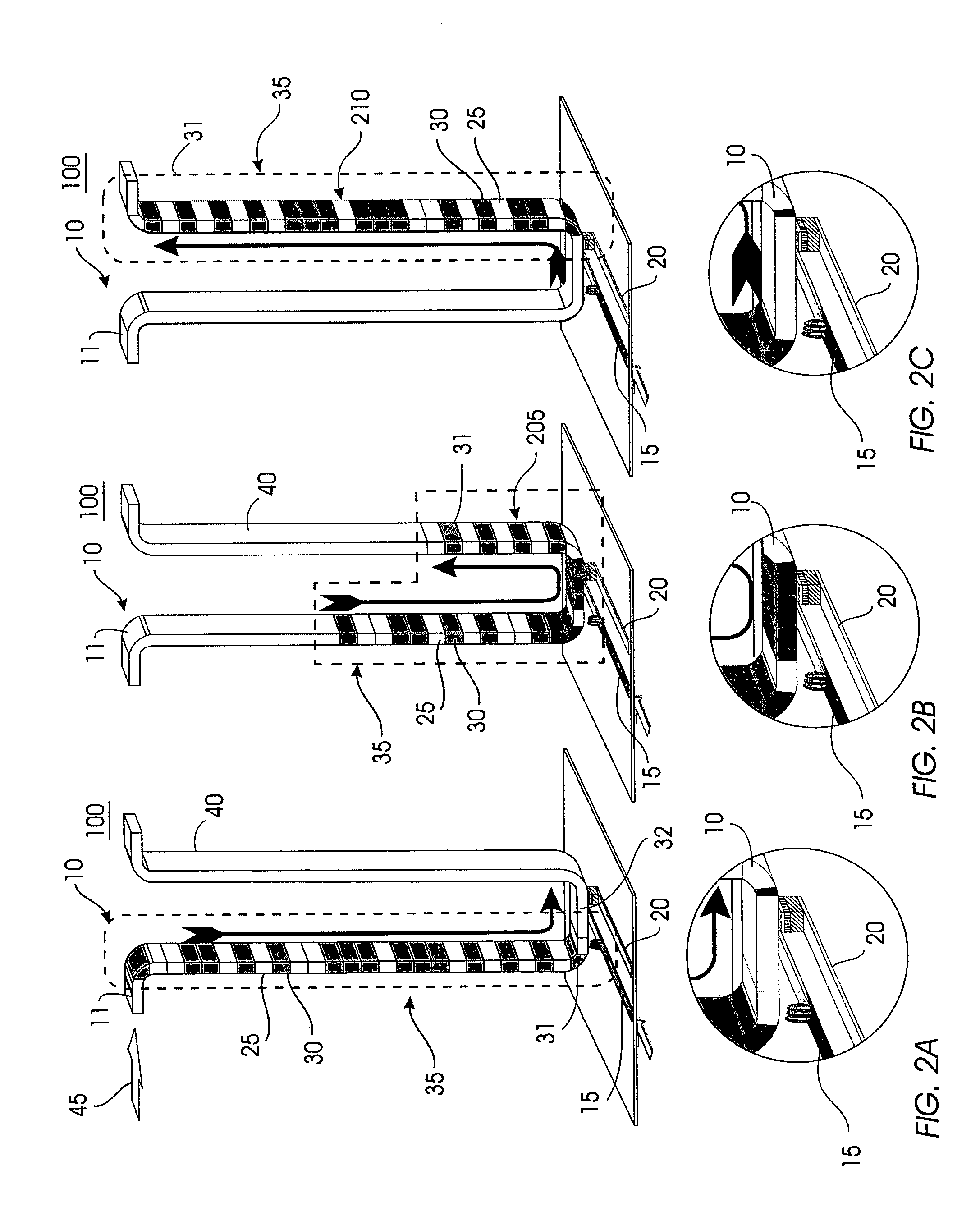
[0050]FIG. 1 (FIGS. 1A and 1B) illustrates an exemplary high-level architecture of a magnetic memory system 100 comprising a magnetic shift register 10 that utilizes a writing device (also referred to herein as writing element) 15 and a reading device (also referred to herein as reading element) 20. Both the reading device 20 and the writing device 15 form a read / write element of system 100.

[0051]The magnetic shift register 10 comprises a fine track 11 made of ferromagnetic material. The track 11 can be magnetized in small sections, or domains, in one direction or another. Information is stored in regions such as domains 25, 30 in the track 11. The order parameter of the magnetic material from which the track is fabricated, that is the magnetization direction or the direction of the magnetic moment, changes from one direction to another. This variation in the direction of the magnetic moment forms the basis for storing information in the track 11.

[0052]In one embodiment, the magneti...


PUM

PropertyMeasurementUnit
timeaaaaaaaaaa
velocitiesaaaaaaaaaa
sizeaaaaaaaaaa

Abstract

A magnetic shift register uses the inherent, natural properties of domain walls in magnetic materials to store data. The shift register uses spin electronics without changing the physical nature of its constituent materials. The shift register comprises a fine track or strip of magnetic materials. Information is stored as domain walls in the track. An electric current is applied to the track to move the magnetic moments along the track past a reading or writing device. In a magnetic material with domain walls, a current passed across the domain wall moves the domain wall in the direction of the current flow. As the current passes through a domain, it becomes “spin polarized”. When this spin polarized current passes through the next domain and across a domain wall, it develops a circle of spin torque. This spin torque moves the domain wall.

Description

PRIORITY CLAIM[0001]The present application is a continuation application under 35 USC 119 of, and claims the priority of non-provisional, U.S. patent application titled “Shiftable Magnetic Shift Register and Method of Using the Same,” Ser. No. 10 / 458,554, which was filed an Jun. 10, 2003, and which issued as U.S. Pat. No. 6,834,005, on Dec. 21, 2004; and is also a continuation application under 35 USC 119 of, and claims the priority of non-provisional, U.S. patent application titled “System and Method for Writing to a Magnetic Shift Register,” Ser. No. 10 / 458,147, which was filed on Jun. 10, 2003 now U.S. Pat. No. 6,898,132 both of these applications are assigned to the same assignee as the present application, and are incorporated herein by reference.FIELD OF THE INVENTION[0002]The present invention generally relates to memory storage systems, and particularly to a memory storage system that uses the magnetic moment of magnetic domains to store data. Specifically, the present inve...

Claims


Application Information

Patent Timeline
Patent Type & Authority Patents(United States)
IPC IPC(8): G11C19/02G11C11/14G11C19/08H01F10/14H01F41/26
CPCG11C11/14G11C19/02G11C19/0841G11C19/0808H01F41/26H01F10/14G11C11/1673G11C11/1675
Inventor PARKIN, STUART S. P.
Owner GLOBALFOUNDRIES U S INC
Why Eureka
Try Eureka