System and method for storing data in an unpatterned, continuous magnetic layer

a magnetic layer and data technology, applied in the field of memory storage systems, can solve the problems of large changes in the magnitude of field required for writing individual devices, the mtj elements are scalded to very small sizes, and the switching fields of these elements become ever more sensitive to the detailed structure of the edges of these devices, so as to achieve higher local magnetic fields and higher densities.

US6970379B2Active Publication Date: 2005-11-29GLOBALFOUNDRIES U S INC
20 Cites 36 Cited by

Patent Information

Authority / Receiving Office
US · United States
Patent Type
Patents(United States)
Current Assignee / Owner
Publication Date
2005-11-29

Smart Images

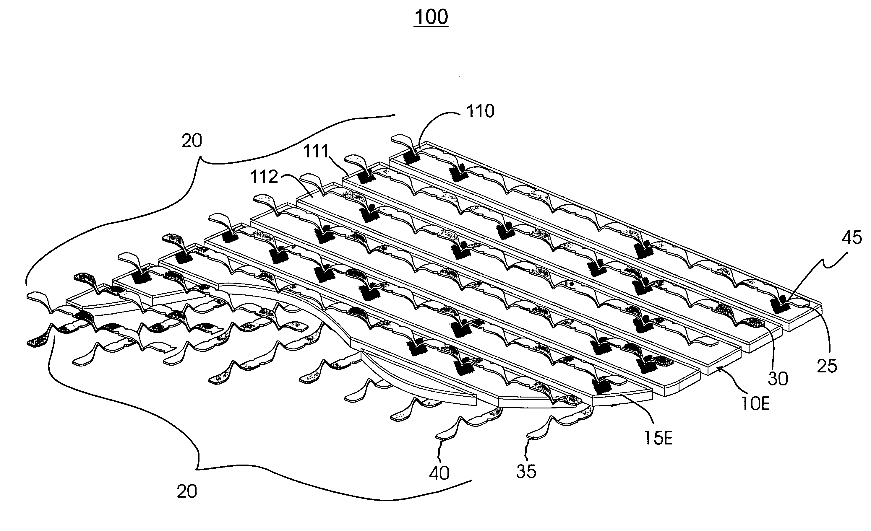
  • Figure 1
    Figure 1
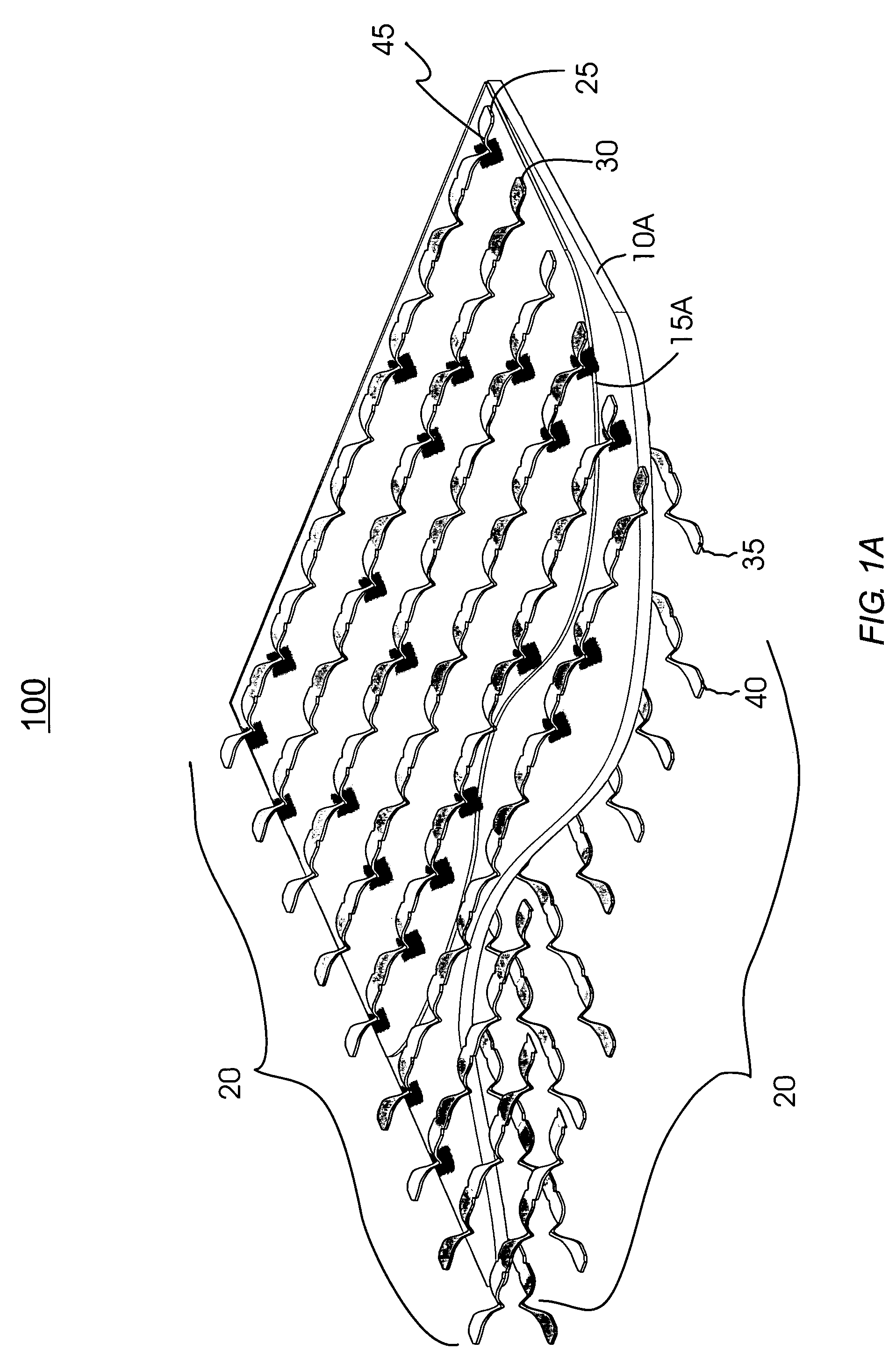
  • Figure 2
    Figure 2
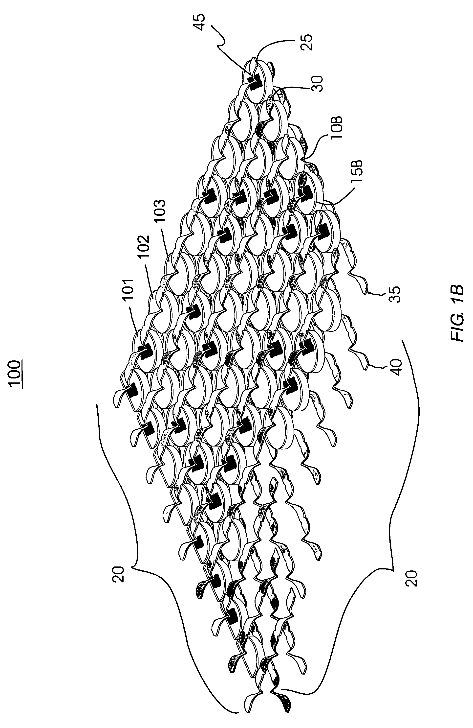
  • Figure 3
    Figure 3
Patent Text Reader

Abstract

Digital information is stored in an unpatterned magnetic film, using the inherent, natural properties of the domain walls in ferromagnetic materials to write data on an unpatterned magnetic film. Data is read from the unpatterned magnetic film using magnetic tunneling junctions (MTJs). To achieve sufficient thermal stability, the magnetic fields required to change the orientation of these magnetic regions may be much larger than can be provided by currents passing through wires. This larger magnetic field is achieved by using the domain wall fringing field generated at the boundary between two magnetic domain walls. The magnetic regions are written by using the fringing fields from magnetic domain walls in neighboring magnetic wires. These wires are brought close to the magnetic storage layer where the magnetic storage regions are to be written.
Need to check novelty before this filing date? Find Prior Art

Description

CROSS-REFERENCE TO RELATED APPLICATIONS

[0001] The present application is related to co-pending U.S. patent applications Ser. No. 10 / 458,554, titled “Shiftable Magnetic Shift Register and Method of Using the Same,” and Ser. No. 10 / 458,147, titled “System and Method for Writing to a Magnetic Shift Register,” both of which were filed on Jun. 10, 2003, and are incorporated herein by reference in their entirety.FIELD OF THE INVENTION

[0002] The present invention generally relates to memory storage systems, and particularly to a memory storage system that uses the magnetic moment of magnetic domains to store data. Specifically, the present invention relates to a system that stores data in an unpatterned, continuous magnetic layer.BACKGROUND OF THE INVENTION

[0003] There is great interest today in magnetic random access memory (MRAM) as a high performance, non-volatile memory using magnetic tunnel junction (MTJ) memory elements. The magnetic tunneling junction comprises two layers of ferromagne...

Examples

Embodiment Construction

[0045]Conventional MRAM architectures involve the use of discrete magnetic memory elements with a particular shape and size that are lithographically patterned by, for example, conventional optical and / or electron beam lithography and etching. Typically, these memory elements are fabricated on top of micro-electronic components, such as transistors and capacitors, which form circuits which are used for the purposes of reading, writing and interrogating the magnetic memory elements.

[0046]These components are formed first, typically on silicon wafers, and then the magnetic memory elements are fabricated, usually by first depositing a continuous film across the wafer which comprises the magnetic memory element. The film is then lithographically patterned into magnetic memory devices of a particular and well defined shape and size which are aligned very precisely with wires or vias which connect these elements to the underlying electronic components.

[0047]Finally, vias and wires are fab...