System and method for storing data in an unpatterned, continuous magnetic layer

a magnetic layer and data technology, applied in the field of memory storage systems, can solve the problems of large changes in the magnitude of field required for writing individual devices, the mtj elements are scalded to very small sizes, and the switching fields of these elements become ever more sensitive to the detailed structure of the edges of these devices, so as to achieve higher local magnetic fields and higher densities.

Active Publication Date: 2005-04-14
GLOBALFOUNDRIES US INC
View PDF20 Cites 88 Cited by
  • Summary
  • Abstract
  • Description
  • Claims
  • Application Information

AI Technical Summary

Benefits of technology

[0028] One advantage of this invention compared to conventional MRAM designs is that the field required to write the magnetic regions in the unpatterned magnetic data storage layer is influenced only by the magnetic properties of this layer and not by the detailed physical structure of a nanopatterned magnetic element. Furthermore, the use of domain wall fringing fields in magnetic writing elements may allow much higher local magnetic fields than are possible to generate from electrical currents passing through non-magnetic wires. This allows for an MRAM that can achieve much higher densities than is possible with conventional cross-point designs.

Problems solved by technology

One of the major problems with MRAM using MJTs is scaling the MTJ elements to very small sizes.
The switching fields of these elements become ever more sensitive to the detailed structure of the edges of these devices as the devices become smaller.
Small variations in shapes and sizes of the MTJs and edge roughness of these devices cause large changes in the magnitude of field required for writing the individual device.
The maximum current is limited ultimately by electro-migration whereby atoms in the wires can be moved by current passing through the wire which can eventually lead to failure of the wire due typically to local necking of the wire which results in an increase in the local current density leading to a runaway process.
Thus, in actual devices the current density must be below this limit, but, even under these circumstances, the current density will be limited by other considerations, including requirements on power dissipation and the size of power transistors on the chip.
However, these devices then become susceptible to thermal upsets due to the super-paramagnetic effect.
The need for such a system has heretofore remained unsatisfied.

Method used


Image

  • System and method for storing data in an unpatterned, continuous magnetic layer
  • System and method for storing data in an unpatterned, continuous magnetic layer
  • System and method for storing data in an unpatterned, continuous magnetic layer

Examples


Embodiment Construction

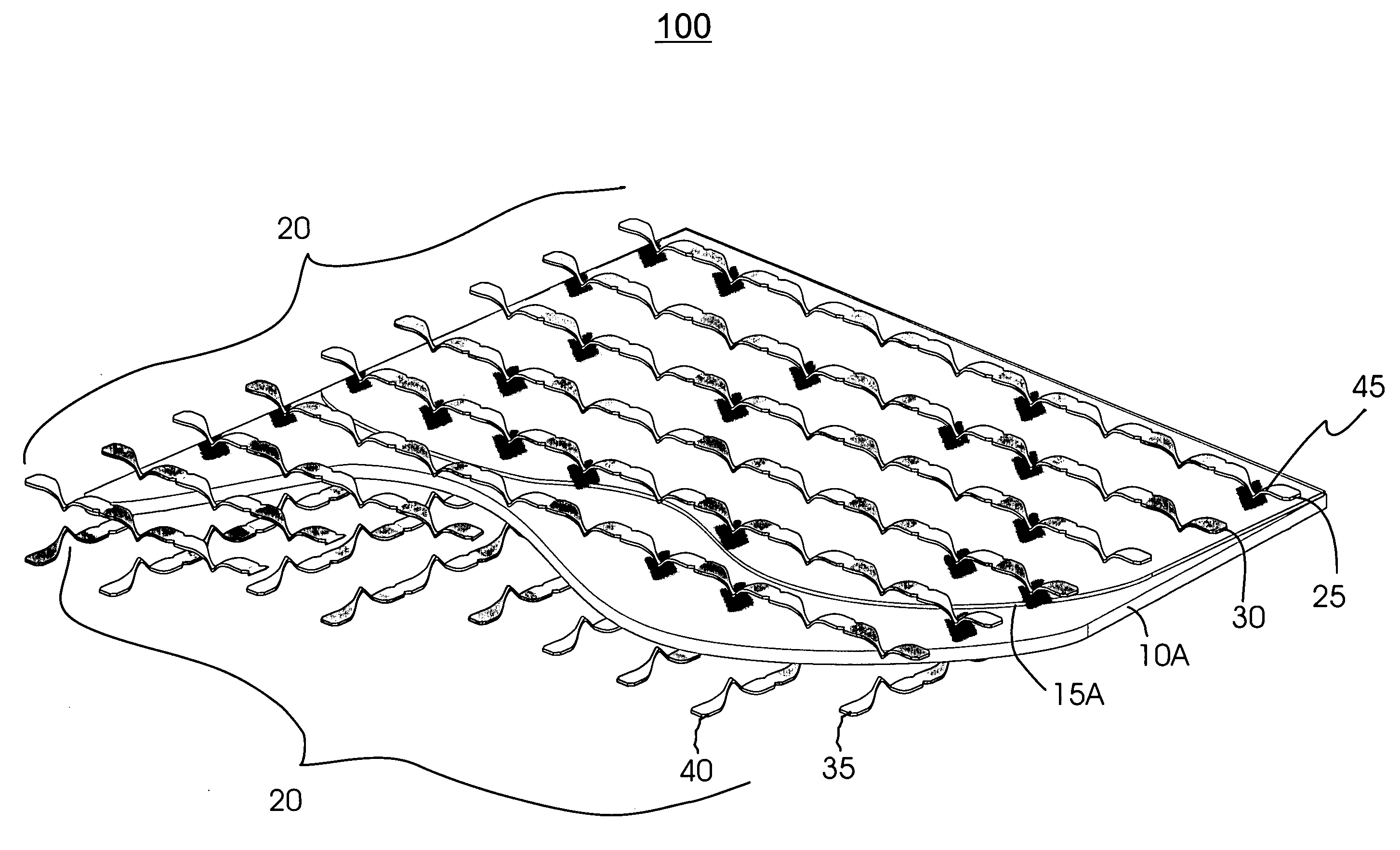
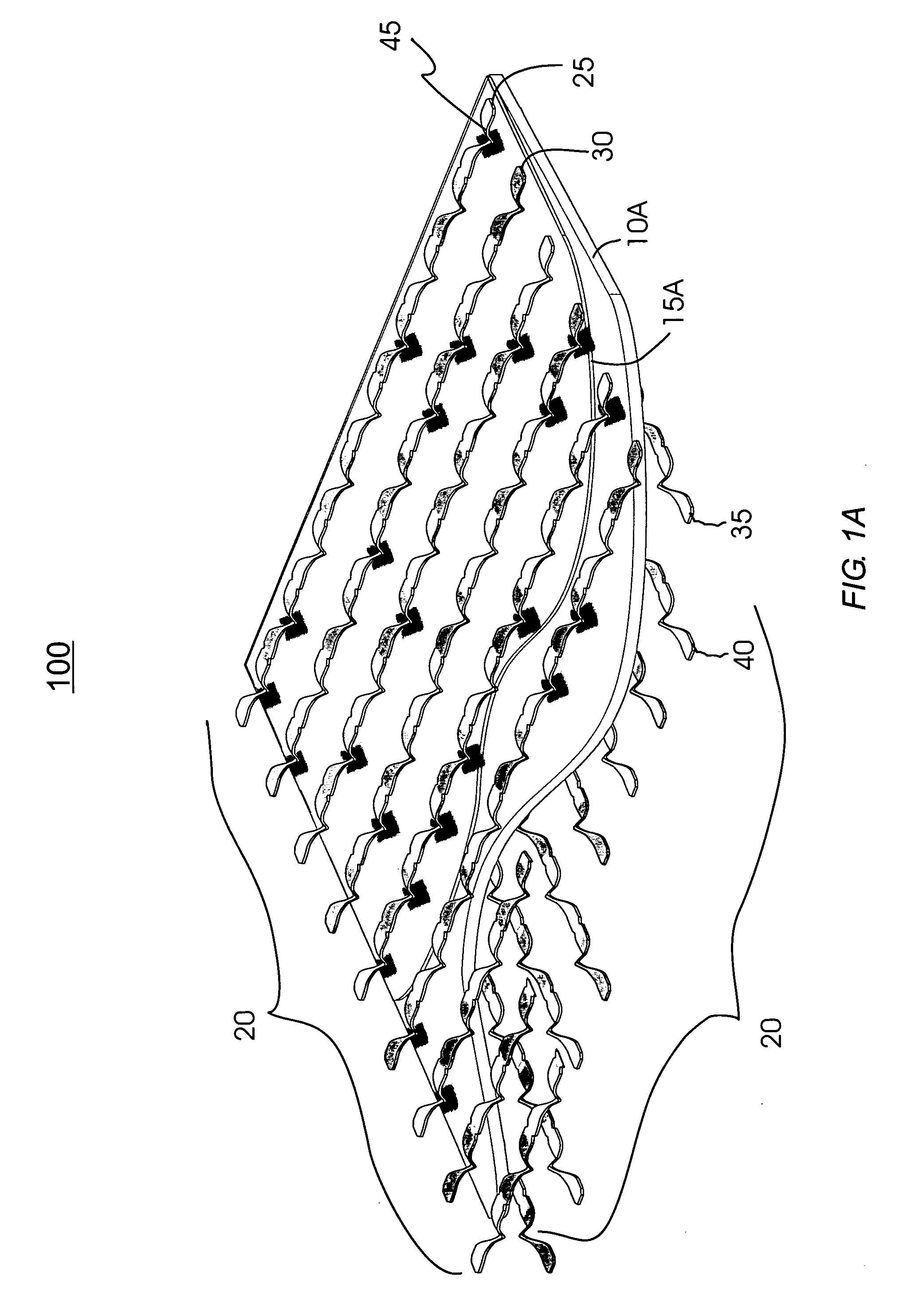
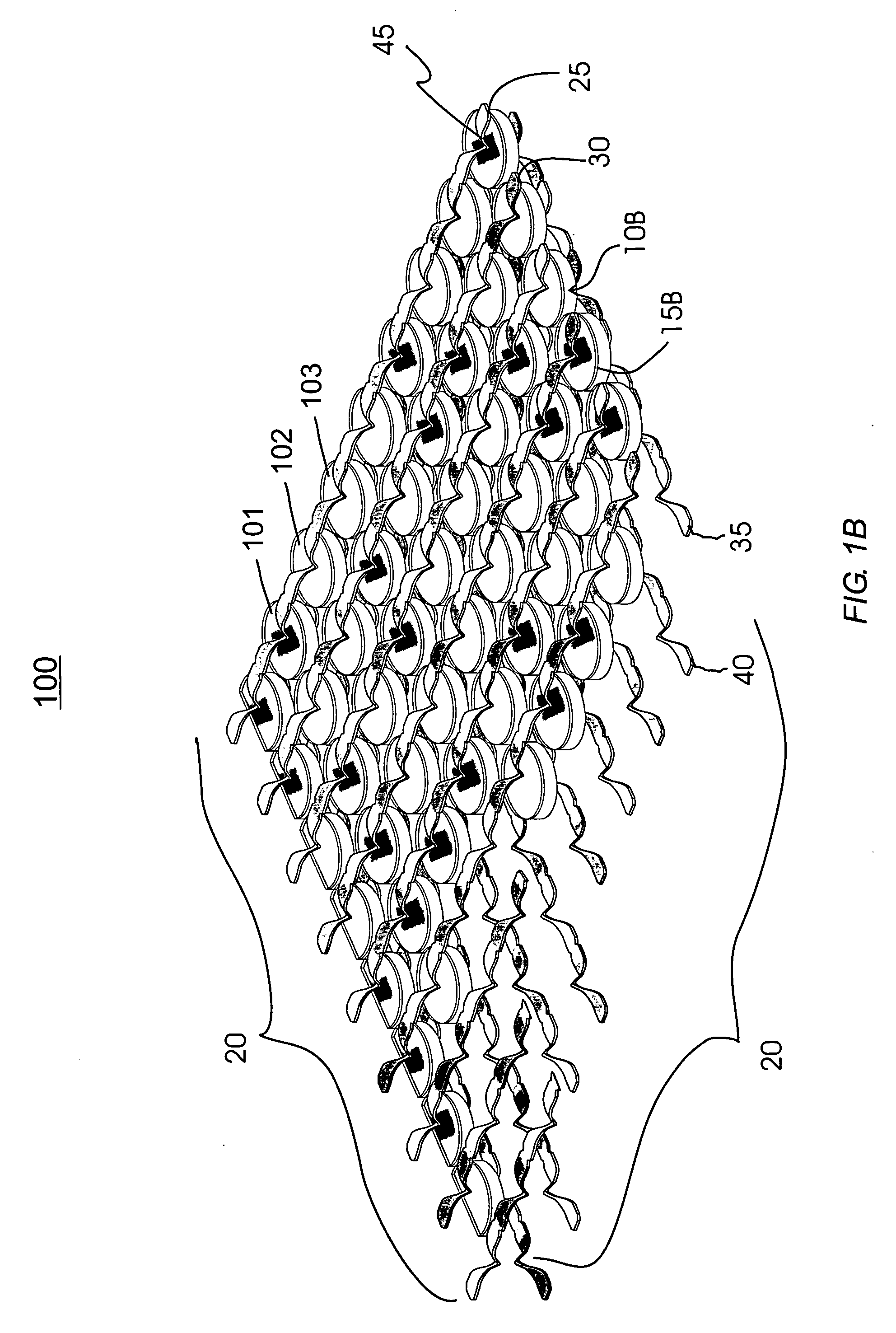
[0045] Conventional MRAM architectures involve the use of discrete magnetic memory elements with a particular shape and size that are lithographically patterned by, for example, conventional optical and / or electron beam lithography and etching. Typically, these memory elements are fabricated on top of micro-electronic components, such as transistors and capacitors, which form circuits which are used for the purposes of reading, writing and interrogating the magnetic memory elements.

[0046] These components are formed first, typically on silicon wafers, and then the magnetic memory elements are fabricated, usually by first depositing a continuous film across the wafer which comprises the magnetic memory element. The film is then lithographically patterned into magnetic memory devices of a particular and well defined shape and size which are aligned very precisely with wires or vias which connect these elements to the underlying electronic components.

[0047] Finally, vias and wires ar...


PUM


Abstract

Digital information is stored in an unpatterned magnetic film, using the inherent, natural properties of the domain walls in ferromagnetic materials to write data on an unpatterned magnetic film. Data is read from the unpatterned magnetic film using magnetic tunneling junctions (MTJs). To achieve sufficient thermal stability, the magnetic fields required to change the orientation of these magnetic regions may be much larger than can be provided by currents passing through wires. This larger magnetic field is achieved by using the domain wall fringing field generated at the boundary between two magnetic domain walls. The magnetic regions are written by using the fringing fields from magnetic domain walls in neighboring magnetic wires. These wires are brought close to the magnetic storage layer where the magnetic storage regions are to be written.

Description

CROSS-REFERENCE TO RELATED APPLICATIONS [0001] The present application is related to co-pending U.S. patent applications Ser. No. 10 / 458,554, titled “Shiftable Magnetic Shift Register and Method of Using the Same,” and Ser. No. 10 / 458,147, titled “System and Method for Writing to a Magnetic Shift Register,” both of which were filed on Jun. 10, 2003, and are incorporated herein by reference in their entirety. FIELD OF THE INVENTION [0002] The present invention generally relates to memory storage systems, and particularly to a memory storage system that uses the magnetic moment of magnetic domains to store data. Specifically, the present invention relates to a system that stores data in an unpatterned, continuous magnetic layer. BACKGROUND OF THE INVENTION [0003] There is great interest today in magnetic random access memory (MRAM) as a high performance, non-volatile memory using magnetic tunnel junction (MTJ) memory elements. The magnetic tunneling junction comprises two layers of fe...

Claims


Application Information

Patent Timeline
Patent Type & Authority Applications(United States)
IPC IPC(8): G11C11/15G11C11/14G11C19/08H01L21/8246H01L27/105H01L43/08
CPCB82Y10/00G11C19/0808G11C11/14
Inventor PARKIN, STUART S. P.
Owner GLOBALFOUNDRIES US INC
Why Eureka
Try Eureka