Bit cell array for preventing coupling effect in read only memory

a technology of read only memory and bit cell array, which is applied in the direction of precision positioning equipment, manufacturing tools, instruments, etc., can solve the problem of reducing the speed of operation

Active Publication Date: 2006-04-18
SAMSUNG ELECTRONICS CO LTD
View PDF8 Cites 17 Cited by
  • Summary
  • Abstract
  • Description
  • Claims
  • Application Information

AI Technical Summary

Problems solved by technology

While data error caused by the coupling effect between bit lines can be prevented in the above-mentioned patents, there is a disadvantage to the disclosed approaches that operational speed is reduced by selectively precharging bit lines using the NMOS multiplexer circuit.

Method used


Image

  • Bit cell array for preventing coupling effect in read only memory
  • Bit cell array for preventing coupling effect in read only memory
  • Bit cell array for preventing coupling effect in read only memory

Examples


Embodiment Construction

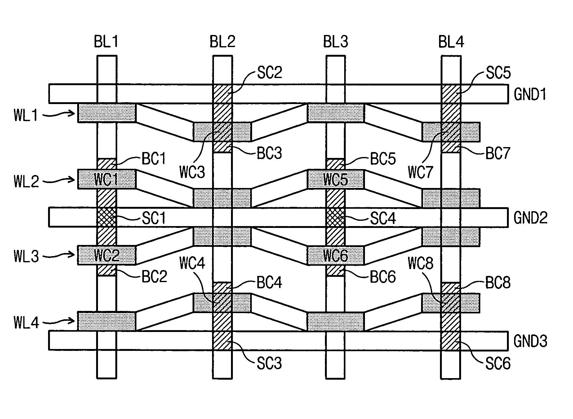
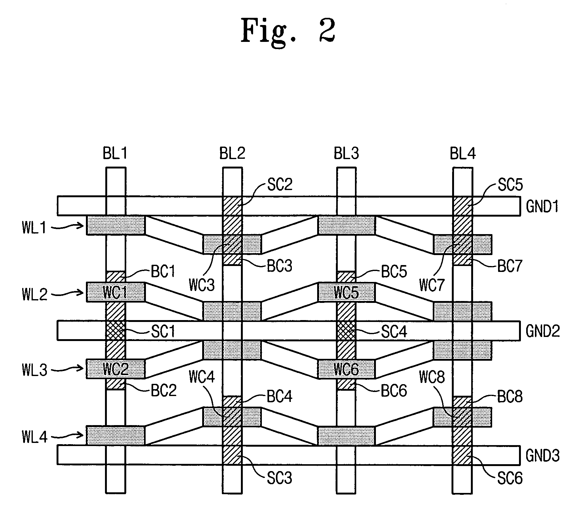
[0024]FIG. 2 is a diagram showing an embodiment of a basic unit bit cell array of a memory unit capable of preventing a coupling effect between adjacent bit lines in a read-only-memory according to the present invention.

[0025]As a matter of convenience, FIG. 2 only shows the bit cell array of a basic unit of a memory cell. An entire bit cell array is structured by repetition of the basic unit bit cell array. As shown in FIG. 2, the basic unit bit cell array includes four bit lines BL1, BL2, BL3 and BL4, four word lines WL1, WL2, WL3 and WL4, three ground lines GND1, GND2 and GND3, and several ROM bit cells (oblique lines in FIG. 2).

[0026]Four bit lines BL1, BL2, BL3 and BL4 are parallel to each other in a first direction.

[0027]Three ground lines GND1, GND2 and GND3 are parallel to each other in a direction perpendicular or vertical to the first direction. Each of the ground lines GND1, GND2 and GND3 has a respective ground voltage.

[0028]Four word lines WL1, WL2, WL3 and WL4 are arra...


PUM


Abstract

The present invention relates to bit cell arrays of read-only-memories, and more specifically, to a bit cell array capable of preventing a coupling effect between adjacent bit lines. In addition, the bit cell array according to the present invention does not require an additional device in order to prevent the coupling effect. In accordance with the present invention, the bit cell array comprising: a plurality of bit lines arranged in a row in a first direction; a plurality of ground lines in a row in a second direction vertical to the first direction; a plurality of word lines arranged with a zigzag line with respect to the second direction; and a plurality of ROM bit cells partially formed at a cross-section point of the bit lines and the word lines. In the meanwhile, the ROM bit cells are arranged with a zigzag line with respect to adjacent bit lines. Additionally, the ROM bit cells comprise a drain terminal, a gate terminal and a source terminal. The drain terminal is connected to one of bit lines, the gate terminal is connected to one of word lines, and the source terminal is connected to one of ground lines.

Description

CROSS-REFERENCE TO RELATED APPLICATIONS[0001]This U.S. non-provisional patent application claims priority under 35 U.S.C. § 119 of Korean Patent Application 2004-02002 filed on Jan. 12, 2004, the entire contents of which are hereby incorporated by reference.BACKGROUND OF THE INVENTION[0002]Read-only-memories (ROMs) as nonvolatile memories are capable of storing data, even with power turned off. In that the ROM is capable of reading the stored data but is incapable of changing it, the ROM is different from Random Access Memories (RAMs) capable of reading and writing data.[0003]FIG. 1 illustrates a portion of a conventional ROM constructed in accordance with the invention. The illustrated ROM is disclosed in U.S. Pat. No. 5,835,421, entitled, “METHOD AND APPARATUS FOR REDUCING FAILURE DUE TO BIT LINE COUPLING AND REDUCING POWER COMSUMPTION IN A MEMORY”.[0004]Referring to FIG. 1, the conventional ROM includes a bit cell array 100. The bit cell array 100 comprises a plurality of bit lin...

Claims


Application Information

Patent Timeline
Patent Type & Authority Patents(United States)
IPC IPC(8): G11C17/00H01L27/10G11C7/02G11C8/14G11C17/12H01L21/8246H01L27/115
CPCG11C7/02H01L27/115G11C8/14G11C17/12H10B69/00B23Q16/02B23Q5/36B23Q5/56
Inventor YON, SANG-HOONLIM, JEUNG-JOO
Owner SAMSUNG ELECTRONICS CO LTD
Why Eureka
Try Eureka