Trench gate laterally diffused MOSFET devices and methods for making such devices

Inactive Publication Date: 2006-04-25
SEMICON COMPONENTS IND LLC
View PDF265 Cites 75 Cited by
  • Summary
  • Abstract
  • Description
  • Claims
  • Application Information

AI Technical Summary

Benefits of technology

[0006]The invention provides a MOSFET device for RF applications that uses a trench gate in place of the lateral gate used in lateral MOSFET devices. The trench gate in the devices of the invention is provided with a single, short channel for high frequency gain. The device of the invention is also provided with an asymmetric oxide in the trench gate, as well as LDD regions that lower the gate-drain capacitance for improved RF performance. Such features allow these devices to maintain the advantages of the LDMOS structure (better linearity), thereby increasing the RF power gain. The trench gate LDMOS of the invention also reduces the hot carrier effects when compared to regular LDMOS devices by reducing the peak electric field and impact ionization. Thus, the devices of the invention will have a better breakdown capability.

Problems solved by technology

The RF vertical (or vertically-diffused) VDMOS structure unfortunately suffers from certain limitations relative to the LDMOS such as high output capacitance (which decreases efficiency), decreased power gain, narrowing of the usable bandwidth, and source inductance that decreases the operating efficiency.
The proposed structure in that patent, unfortunately suffers from several setbacks.

Method used


Image

  • Trench gate laterally diffused MOSFET devices and methods for making such devices
  • Trench gate laterally diffused MOSFET devices and methods for making such devices
  • Trench gate laterally diffused MOSFET devices and methods for making such devices

Examples


Embodiment Construction

[0015]The following description provides specific details in order to provide a thorough understanding of the invention. The skilled artisan, however, would understand that the invention can be practiced without employing these specific details. Indeed, the invention can be practiced by modifying the illustrated system and method and can be used in conjunction with apparatus and techniques conventionally used in the industry. For example, the MOSFET devices are described for RF applications, but could be used in non-RF applications such as switching.

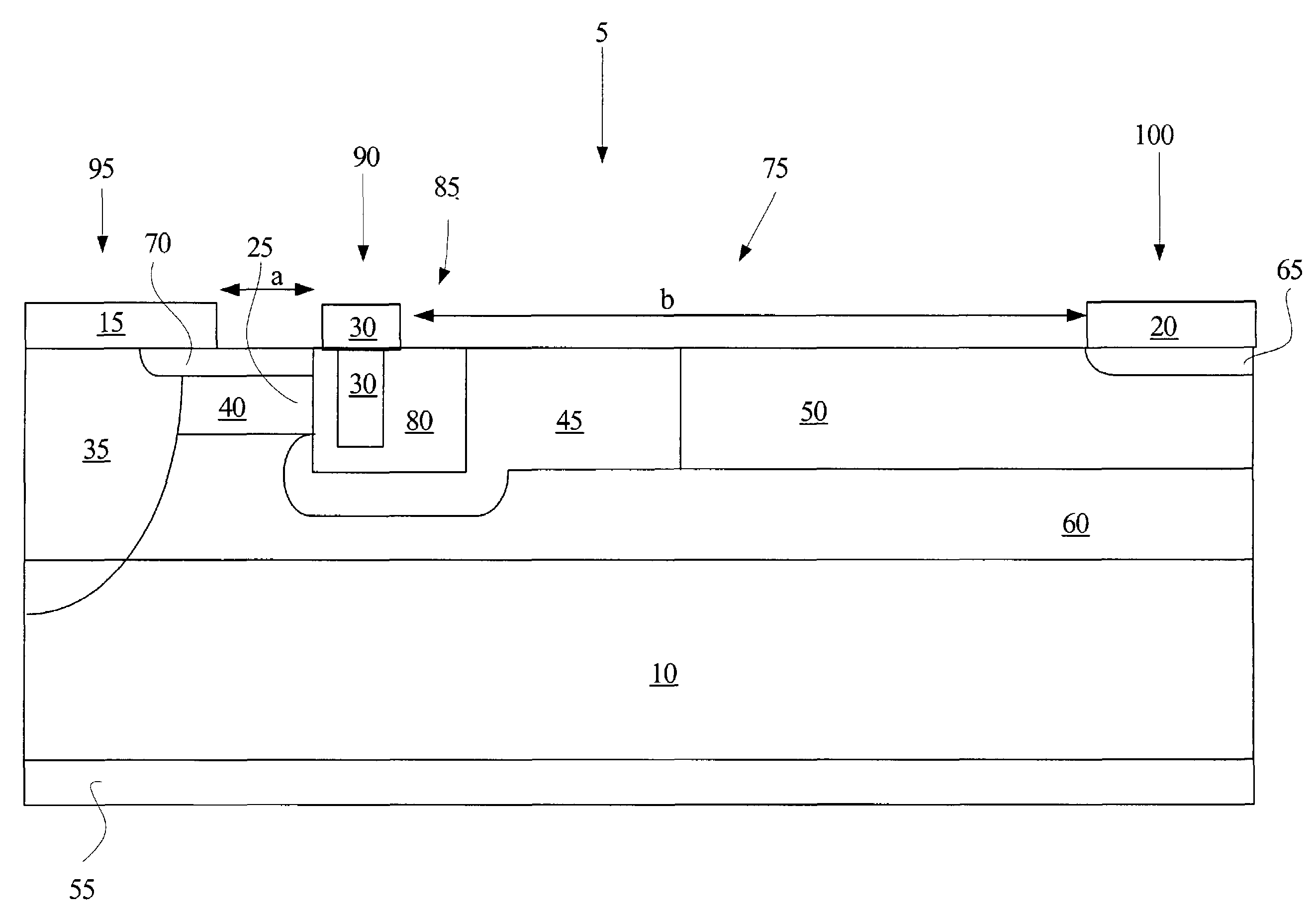
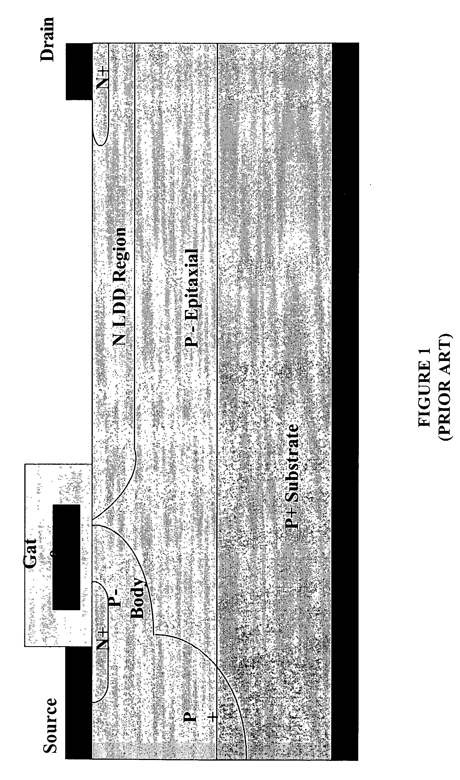
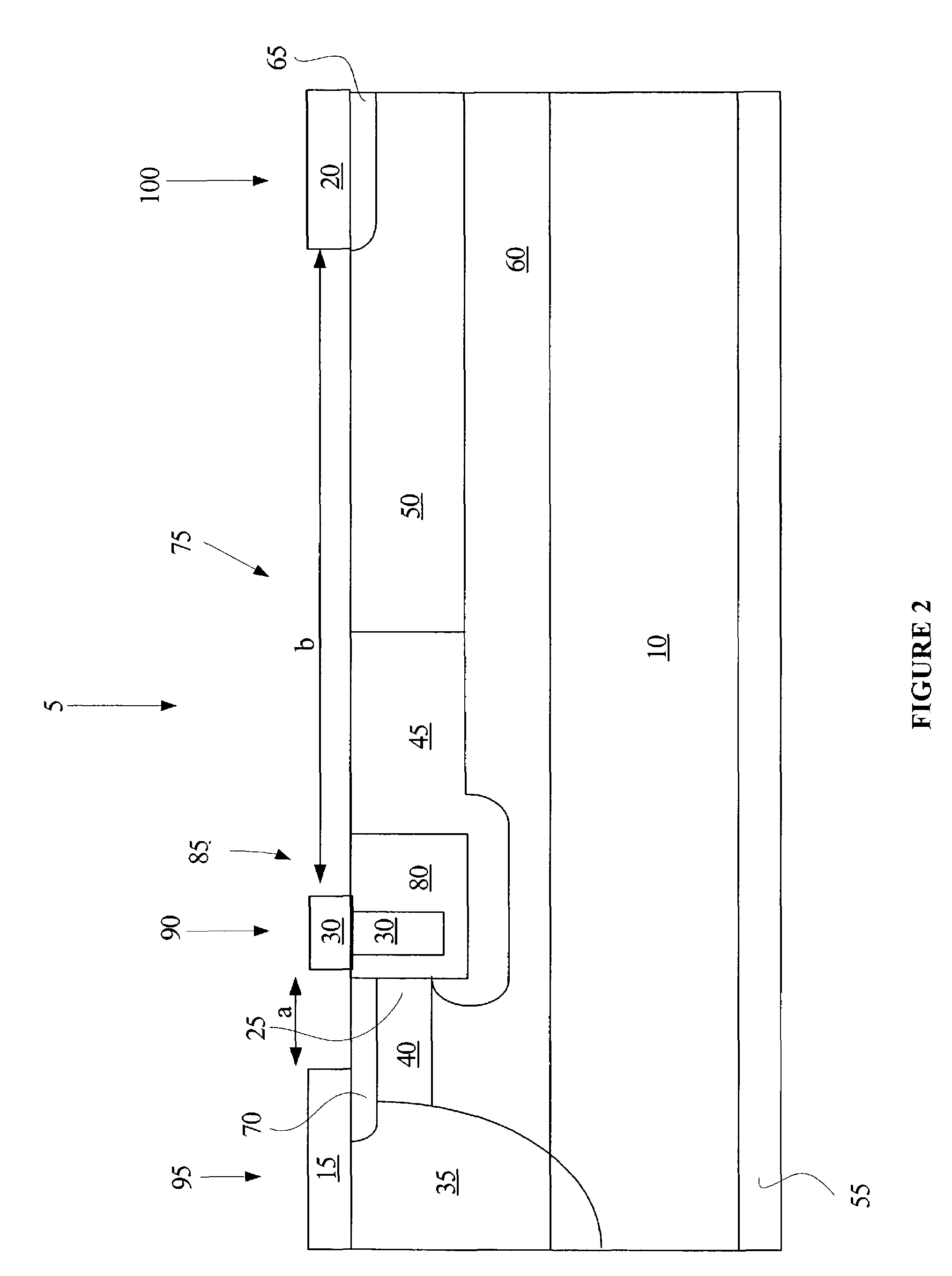
[0016]As noted above, the invention generally comprises a structure that combines the benefits of the LDMOS structure (i.e., a low gate-to-drain capacitance and a good linearity) with the benefits of a short gate channel. Thus, any structure that combines theses feature can be employed in the invention. In one aspect of the invention, these benefits are combined by using a trench gate laterally-diffused MOSFET device as described below. ...


PUM


Abstract

A MOSFET device for RF applications that uses a trench gate in place of the lateral gate used in lateral MOSFET devices is described. The trench gate in the devices of the invention is provided with a single, short channel for high frequency gain. The device of the invention is also provided with an asymmetric oxide in the trench gate, as well as LDD regions that lower the gate-drain capacitance for improved RF performance. Such features allow these devices to maintain the advantages of the LDMOS structure (better linearity), thereby increasing the RF power gain. The trench gate LDMOS of the invention also reduces the hot carrier effects when compared to regular LDMOS devices by reducing the peak electric field and impact ionization. Thus, the devices of the invention will have a better breakdown capability.

Description

FIELD OF THE INVENTION[0001]The invention generally relates to methods for fabricating integrated circuits (ICs) and semiconductor devices and the resulting structures. More particularly, the invention relates to metal oxide semiconductor field effect transistor (MOSFET) devices and methods for making such devices. Even more particularly, the invention relates to trench gate laterally-diffused MOSFET devices and methods for making such devices.BACKGROUND OF THE INVENTION[0002]In IC fabrication, devices such as transistors may be formed on a semiconductor wafer or substrate, which is typically made of silicon. MOSFET devices are widely used in numerous electronic apparatus, including automotive electronics, disk drives and power supplies. Generally, these apparatus function as switches and are used to connect a power supply to a load.[0003]One of the applications in which MOSFET devices have been used is for radio frequency (RF) applications. Such “RF” MOSFET devices generally utiliz...

Claims


Application Information

Patent Timeline
IPC IPC(8): H01L21/336H01L21/8238H01L29/76H01L29/94H01L31/062H01L29/423H01L29/78
CPCH01L29/0847H01L29/4175H01L29/4236H01L29/42368H01L29/66621H01L29/66659H01L29/7831H01L29/7834H01L29/7835
Inventor WILSON, PETER H.SAPP, STEVENTHORNTON, NEILL
Owner SEMICON COMPONENTS IND LLC
Why Eureka
Try Eureka