Process for manufacturing MOS semiconductor device having inactive zone with alternating thickness silicon oxide layer

Inactive Publication Date: 2004-10-28
STMICROELECTRONICS SRL
View PDF4 Cites 0 Cited by
  • Summary
  • Abstract
  • Description
  • Claims
  • Application Information

AI Technical Summary

Benefits of technology

[0013] The present invention makes it possible to form a high efficiency MOS semiconductor device that has a lower gate-drain capacitance in the inactive zones such as the gate-pad or the gate-bus.

Problems solved by technology

Such factors, in the radio frequency devices, must be researched in the presence of the parasitic capacitances and in problems linked to the main physic-structural parameters, as the problem related to the power dissipation of the MOS technology device in the stationary state which is linked to the resistance of the device in the on state (Rdson).

Method used


Image

  • Process for manufacturing MOS semiconductor device having inactive zone with alternating thickness silicon oxide layer
  • Process for manufacturing MOS semiconductor device having inactive zone with alternating thickness silicon oxide layer
  • Process for manufacturing MOS semiconductor device having inactive zone with alternating thickness silicon oxide layer

Examples


Embodiment Construction

[0023] Preferred embodiments of the present invention will be described in detail hereinbelow with reference to the attached drawings.

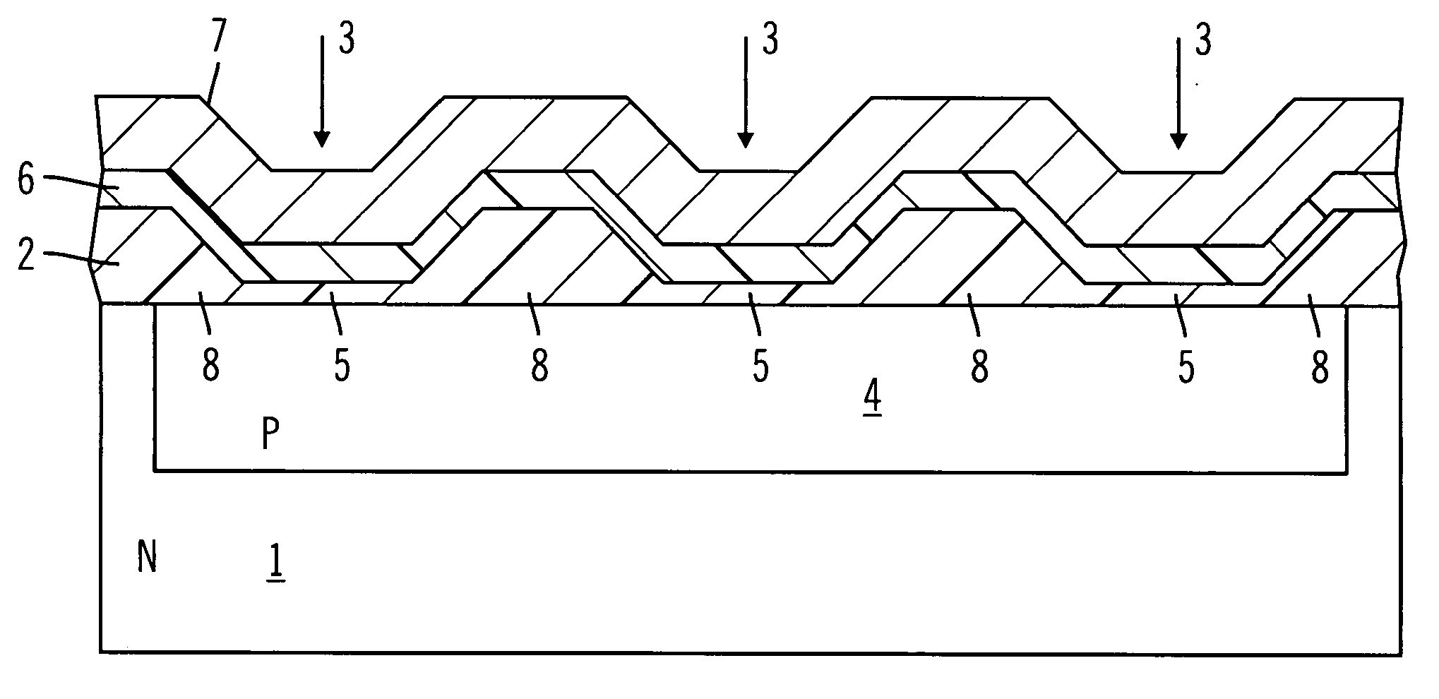
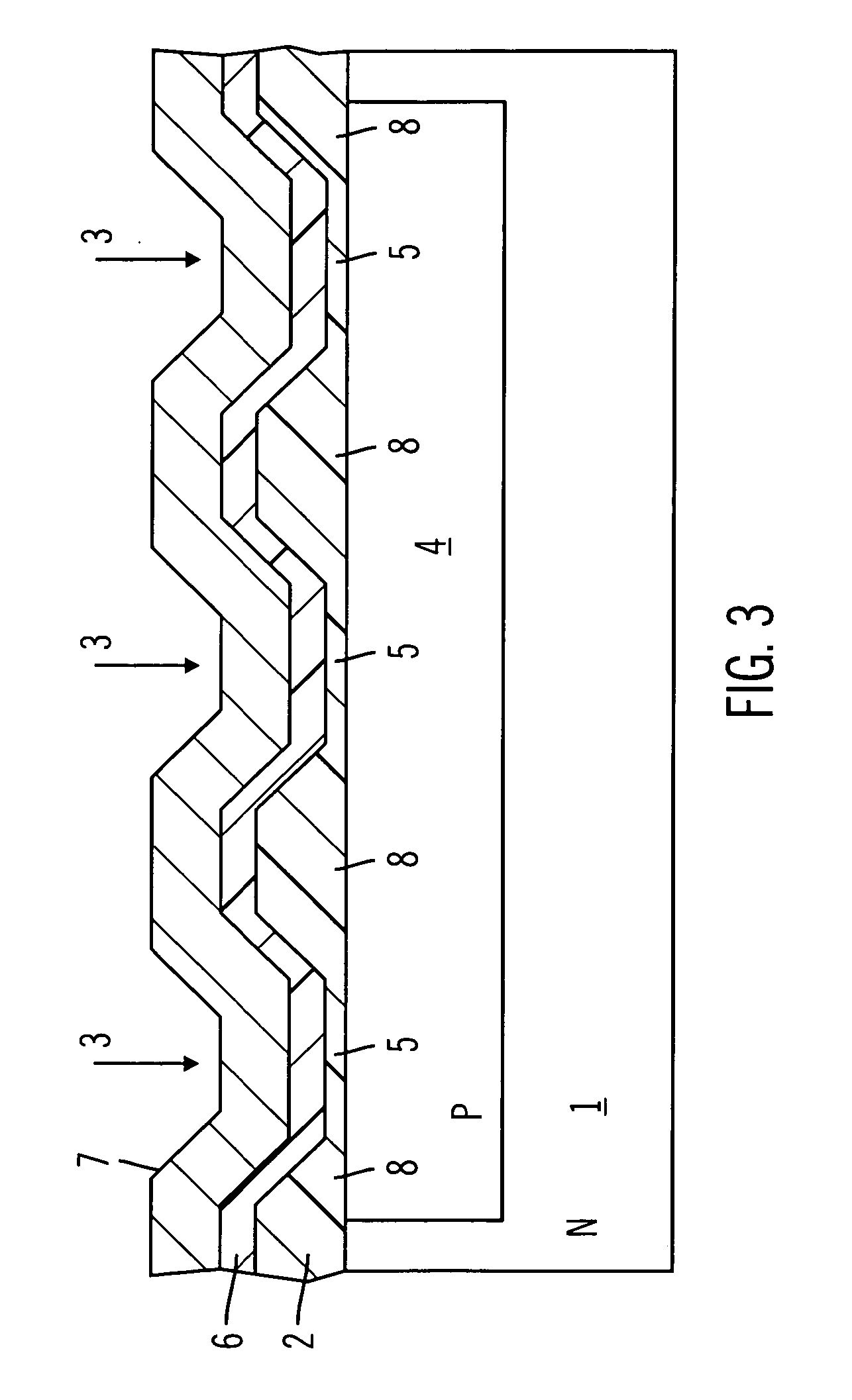
[0024] FIG. 3 shows an inactive zone of a MOS semiconductor device according to a preferred embodiment of the present invention. Such inactive zone, which is destined to become a gate-pad or a gate-bus for the output or the input of the signals, includes an N-type semiconductor substrate having in turn an N-type epitaxial layer 1 which is connected to the drain terminal. A deposition of a field oxide layer 2 (for example with a thickness of 10K angstroms) occurs over a top surface of the epitaxial layer 1, which successively, after appropriate masking, is attached and removed in certain zones 3.

[0025] Under the zones 3, P-type semiconductor wells are formed using a P-type dopant implant and, after a further thermal diffusion step to allow merging of the wells, one P-type region 4 is formed which is connected with the source terminal of the device. Suc...


PUM


Abstract

A MOS semiconductor device formed on a substrate of a first conductivity type is provided. The device includes active zones for elementary active elements, and at least one inactive zone suitable for electric signal input or output. The substrate is connected with the drain terminal of the device, and at least one of the elementary active elements includes a body region of a second conductivity type that is connected with the source terminal of the device. The at least one inactive zone includes a semiconductor region of the second conductivity type formed in the substrate and adjacent a surface of the substrate, a conductive layer located over the semiconductor region, and a silicon oxide layer located between the semiconductor region and the conductive layer. The silicon oxide layer has alternating first zones and second zones that are contiguous to each other, with the first zones having a greater thickness than the second zones.

Description

CROSS-REFERENCE TO RELATED APPLICATIONS[0001] This application is a divisional of application Ser. No. 10 / 251,907, filed Sep. 20, 2002, now U.S. Pat. No.______, which is based upon and claims priority from prior European Patent Application No. 01-830599.5, filed Sep. 21, 2001. The entire disclosures of application Ser. No. 10 / 251,907 and European Patent Application No. 01-830599.5 are herein incorporated by reference.BACKGROUND OF THE INVENTION[0002] 1. Field of the Invention[0003] The present invention relates to semiconductor devices, and more specifically to a high efficiency MOS semiconductor device and to a process for manufacturing the same.[0004] 2. Description of Related Art[0005] In electronic devices, such as those for radio frequency applications, the signals must be treated so as to prevent alteration of the same inside the device. Therefore, in the devices all the factors that can bring about a perturbation of the signal waveform or which can add noise to the signal mus...

Claims


Application Information

Patent Timeline
IPC IPC(8): H01L21/336H01L29/08H01L29/10H01L29/423H01L29/78
CPCH01L29/0847H01L29/1095Y10S438/981H01L29/66712H01L29/7802H01L29/42368
Inventor SCHILLACI, ANTONINOPONZIO, PAOLA MARIA
Owner STMICROELECTRONICS SRL
Why Eureka
Try Eureka