Apparatus for measuring of thin dielectric layer properties on semiconductor wafers with contact self aligning electrodes

a technology of contact self-aligning electrodes and electrodes, which is applied in the direction of individual semiconductor device testing, measurement devices, instruments, etc., can solve the problems of not meeting the requirements of probes, plastically deformable probes may not suit well to a limited size, and all the techniques listed in references [1–4] may not suit well the challenges, etc., to achieve stable measurement conditions and repeatability

Inactive Publication Date: 2006-04-25
APPLEJACK 199 +1
View PDF15 Cites 17 Cited by
  • Summary
  • Abstract
  • Description
  • Claims
  • Application Information

AI Technical Summary

Benefits of technology

[0006]With one electrical means applied to the conductive chuck that firmly supports the wafer and another electrical means applied to the probe tip deposited on the dielectric layer of the wafer the capacitance-voltage (C-V), conductance-voltage (G-V), conductance-frequency (G-F) and current-voltage (I-V) types of electrical stimuli are applied to the wafer at any probe tip location. The measured stimuli reactions allow characterization of dielectric layers on semiconductor wafers and semiconductor substrate interfaces to the dielectric layers while keeping the measurements conditions stable and repeatable at any location on the wafer.

Problems solved by technology

The greatest challenges for the measurements of dielectric layers properties represent product wafers where limited test areas sizes, exact locations of test sites and extraordinary precautions in handling and protecting the wafers are imperative.
All of the techniques listed in References [1–4] may not suit well the challenges urged by the necessity to characterize thin dielectric layers on product wafers.
Plastically deformable probes may not suit well to a limited size and exact positioning of the probe tip at the test site on product wafers.
Mercury probe does not meet the requirements of non-contamination, while elastically deformable probe tips (References [1,2]) may introduce uninvited excessive pressure on dielectric and even destroy the dielectric layer that reaches several tens of Angstrom thickness for modern technologies.

Method used


Image

  • Apparatus for measuring of thin dielectric layer properties on semiconductor wafers with contact self aligning electrodes
  • Apparatus for measuring of thin dielectric layer properties on semiconductor wafers with contact self aligning electrodes
  • Apparatus for measuring of thin dielectric layer properties on semiconductor wafers with contact self aligning electrodes

Examples


Embodiment Construction

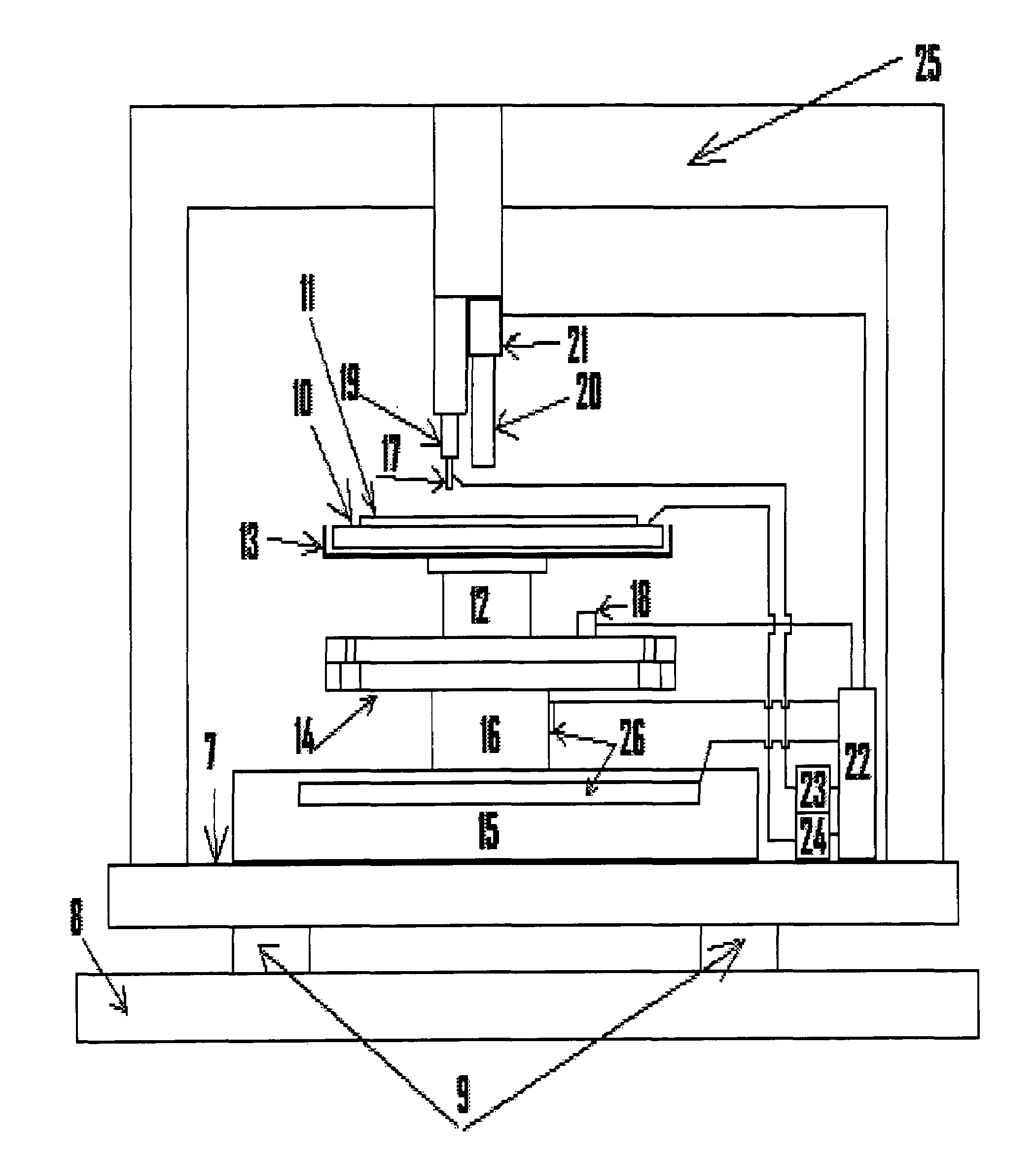
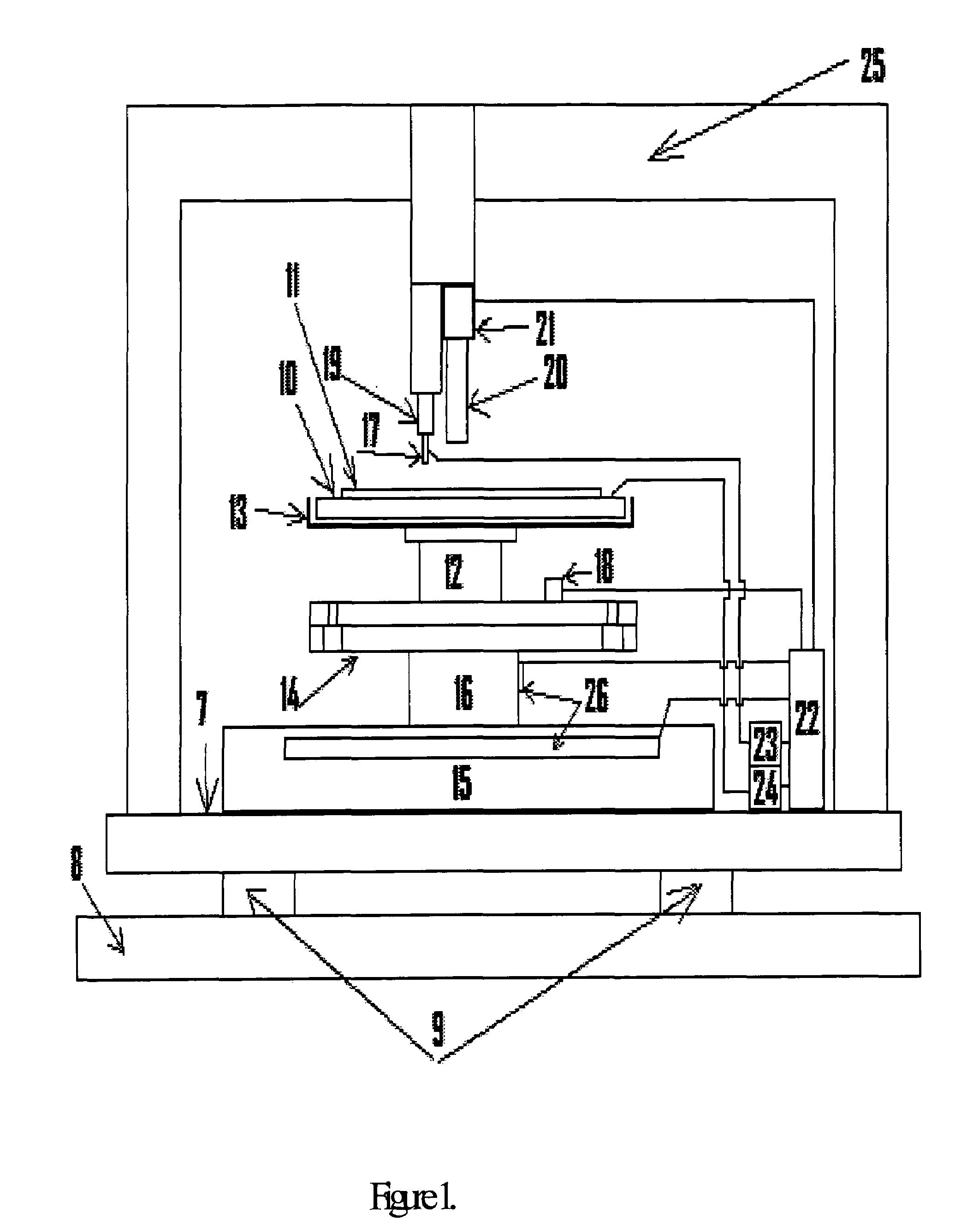
[0009]A side view of the invented apparatus comprising the invented probe 17 is depicted in FIG. 1. A massive bridge 25 is mounted on a platform 7 that is isolated from the vibrations of the supporting frame 8 via active vibration isolation units 9 known in the art. The conductive vacuum chuck 10, known in the art, with a semiconductor finish over the surface where the wafer 11 is placed, is movable along the Z-axis (vertically up and down) by an actuator 12. The deviations of the chuck surface from an ideal plane are ±5 micrometer. The chuck is contained inside an electromagnetic shield 13. The actuator 12 for the chuck 10 is mounted on an adaptor plate 14 that allows adjustment of the chuck surface to horizontal. The quality of the chuck alignment and inspection of chuck surface variations is accomplished via measuring reflections of light from the chuck surface with optical equipment mounted to the massive bridge 25. The adaptor plate 14 is mounted at the top of X (15) and Y (16)...


PUM


Abstract

The invention relates to metrology of thin dielectric layers on semiconductor wafers, interfaces of dielectric layers to the wafer substrates and substrates properties of semiconductor wafers. The invention allows measurement of the metrology data for thin dielectric layers on semiconductor wafers electrically via using contact electrodes that align their contact surface to the wafer surface locally at the measurement sites.

Description

BACKGROUND OF THE INVENTION[0001]Detailed knowledge of thickness and electrical properties of thin oxide (dielectric) layers on semiconductor wafers and semiconductor substrate interfaces to these layers is crucial in predicting device parameters that could be fabricated using any given semiconductor technology. Characterization of dielectric layers and their interfaces to the substrates may be needed at different stages of production from blank wafers to product wafers. The greatest challenges for the measurements of dielectric layers properties represent product wafers where limited test areas sizes, exact locations of test sites and extraordinary precautions in handling and protecting the wafers are imperative.[0002]The most successful solutions for the measurement of the above dielectric layer properties known in the art are offered by contact methods with one electrical means applied to the bottom surface of the wafer and another electrical means applied to the measurement site...

Claims


Application Information

Patent Timeline
Patent Type & Authority Patents(United States)
IPC IPC(8): G01R31/26
CPCG01R31/2831G01R31/2648H01L21/6838
Inventor SOUCHKOV, VITALIFAIFER, VLADIMIRHUANG, VICTORFUKSHANSKY, EUGENEARTJOMOV, ALEXANDERSKLJARNOV, ANATOLI
Owner APPLEJACK 199
Why Eureka
Try Eureka