Eureka AIR delivers breakthrough ideas for toughest innovation challenges, trusted by R&D personnel around the world.

Nonvolatile semiconductor memory device

a semiconductor memory and nonvolatile technology, applied in semiconductor devices, digital storage, instruments, etc., can solve the problems of rapid cooling operation necessary for bringing the nonvolatile recording material layer into the amorphous state, changes in the conditions of rewriting, and difficulty in rewriting. the effect of stable conditions

Inactive Publication Date: 2009-06-04
KINOSHITA MASAHARU +7
View PDF2 Cites 28 Cited by
  • Summary
  • Abstract
  • Description
  • Claims
  • Application Information

AI Technical Summary

Benefits of technology

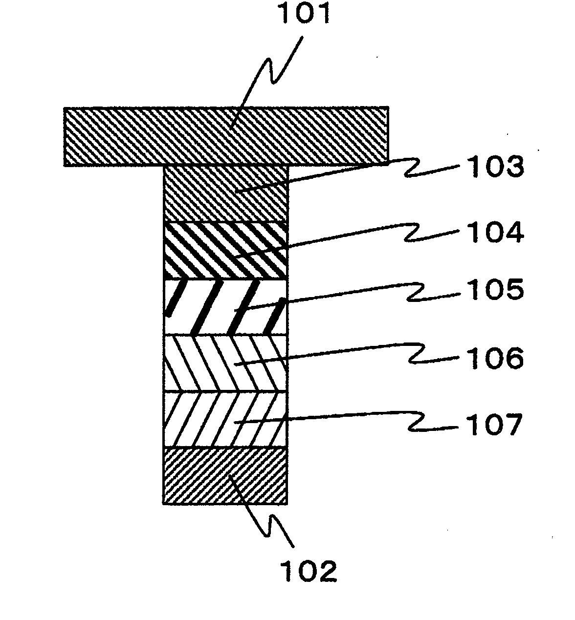
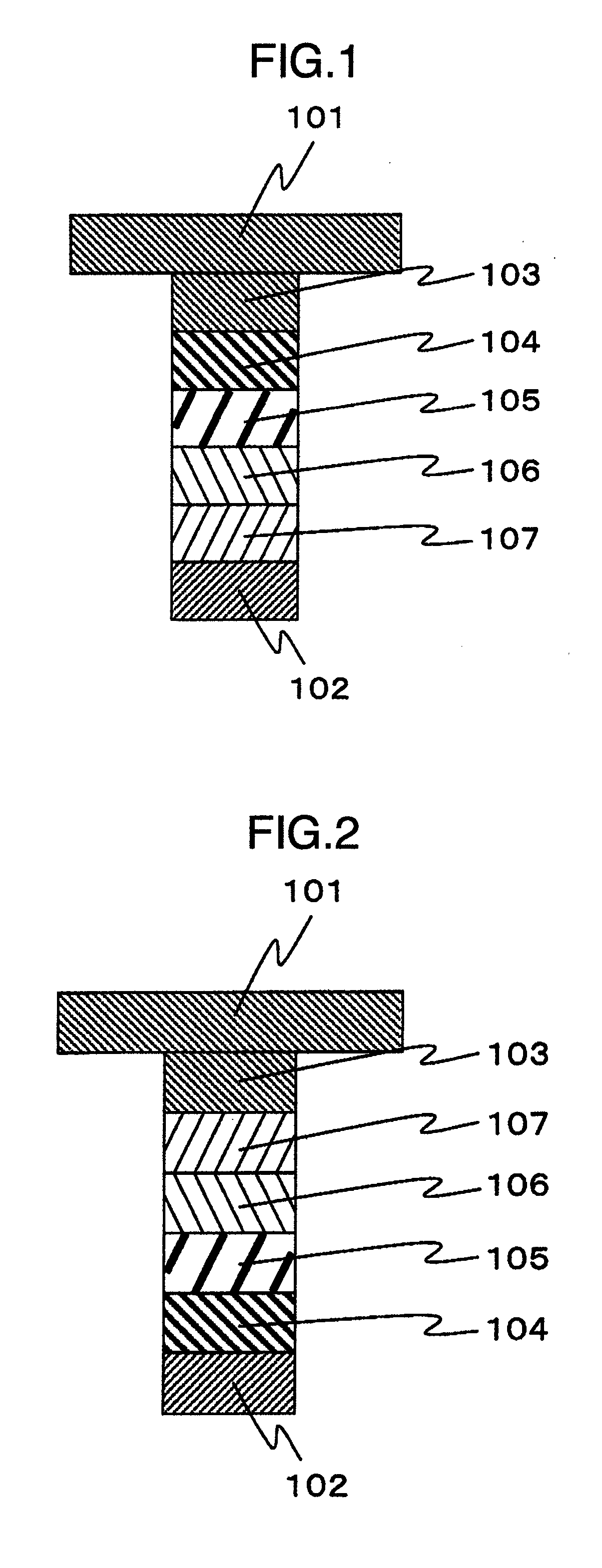
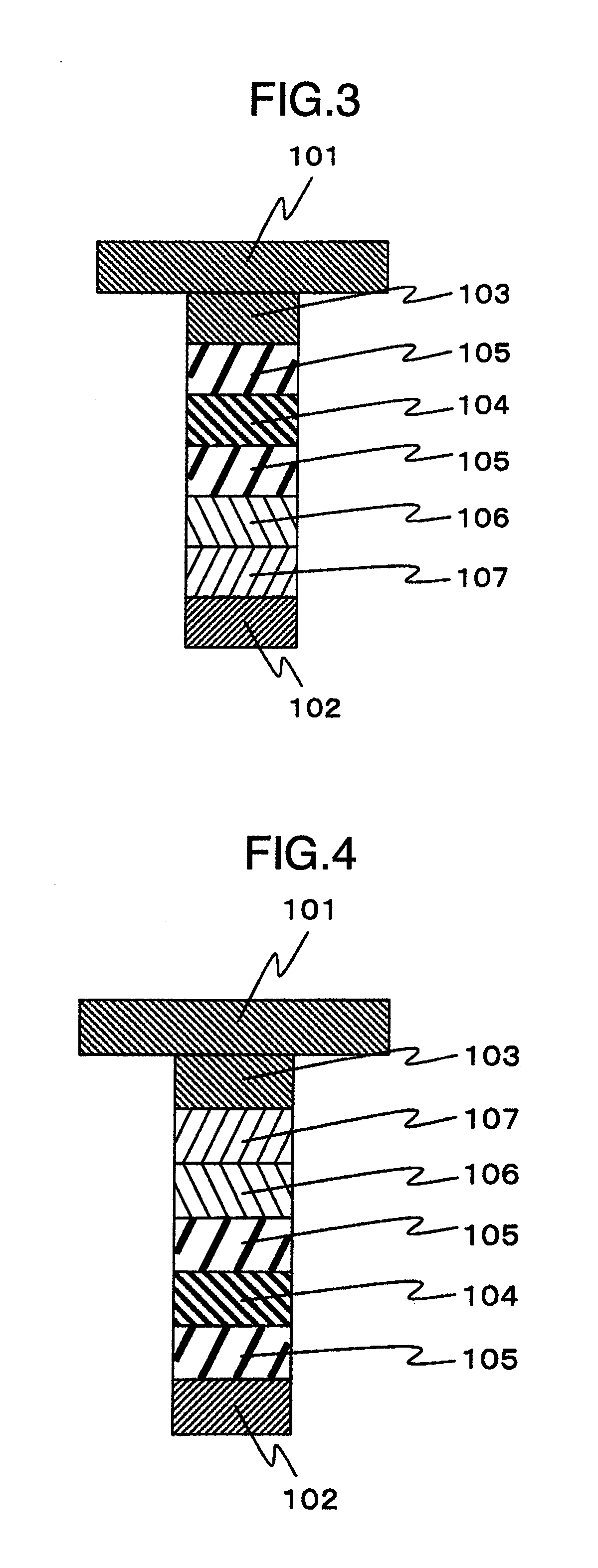
"The present invention provides a phase change memory device that prevents the diffusion of atoms from adjacent layers and facilitates rapid cooling for realizing the amorphous state. The device includes a nonvolatile recording material layer and a selector element between first and second electrodes, with a semiconductor layer containing an element identical with that contained in the nonvolatile recording material layer. The invention allows for stable conditions for rewriting and achieves a high number of rewriting operations with a short rewrite time."

Problems solved by technology

Therefore, as the number of times of the rewriting operation is larger, more atoms constituting a film adjacent to the nonvolatile recording material layer diffuse from that adjacent film into the nonvolatile recording material layer, with a disadvantageous result that conditions for the rewriting are changed.
In this structure, however, diffusion of metal elements from the metal film into the nonvolatile recording material layer may take place, which may lead to changes in conditions for rewriting.
In this structure, however, a rapid cooling operation necessary for bringing the nonvolatile recording material layer into the amorphous state may be difficult.

Method used


Image

  • Nonvolatile semiconductor memory device
  • Nonvolatile semiconductor memory device
  • Nonvolatile semiconductor memory device

Examples


embodiment 1

[0067]A method of manufacturing a memory cell of a nonvolatile memory will be described in detail with reference to the accompanying drawings. Throughout the drawings, members having similar functions are denoted by the same reference symbols and description of the similar members will not be repeated.

[0068]In the description of the following embodiments, generally, explanation of similar or same parts will not be repeated except when it is particularly necessary. With respect to the drawings referred to in connection with the described embodiments, cross-sectional views may not be provided with hatching for clarity of illustration, and plan views may be provided with hatching for clarity of illustration.

[0069]In this embodiment, as shown in FIG. 5, a memory cell is formed on a semiconductor substrate 201. The semiconductor substrate 201 is not only for a nonvolatile memory but also for a peripheral circuit to be formed therein for operating a memory matrix of the nonvolatile memory...

embodiment 2

[0105]In this embodiment, as shown in FIG. 22, memory cells are formed on a semiconductor substrate 201. The semiconductor substrate 201 is not only for a nonvolatile memory but also for a peripheral circuit to be fabricated therein for operating the memory matrix of the nonvolatile memory. The peripheral circuit may be fabricated by the use of the conventional CMOS technology. The positional relationship between the peripheral circuit and the memory matrix may be similar to that in Embodiment 1.

[0106]Referring back to FIG. 22 showing a structure at a step in which, on a semiconductor substrate 201, a first metal connection conductor layer 202, a nonvolatile recording material layer 207, a semiconductor layer 206, a second amorphous silicon layer 204 and a first amorphous silicon layer 251 are formed, in the described order. The first metal connection conductor layer 202 is made of tungsten and is formed by sputtering. More preferably, the layer 202 should be made of, for example, a...

embodiment 3

[0125]FIG. 31 is a perspective view of a semiconductor memory device, in which, on a semiconductor substrate 201, first metal connection conductor layers 210 serving as word lines in a memory matrix, pillar-shaped multi-layer films PU 5, third metal connection conductor layers 226 serving as bit lines in the memory matrix and insulating materials 229 and 228 are formed in a manner similar to that described in connection with Embodiment 1 with reference to FIGS. 5 to 18. Each of the multi-layer films PU 5 includes first and second poly-silicon layers 220 and 221, a semiconductor layer 222, a nonvolatile recording material layer 223, another semiconductor layer 222 and a second metal connection conductor layer 224.

[0126]The provision of the semiconductor layers leads to prevention of the degradation of the nonvolatile recording material layers stemming from the heat cycles at repetitive writing on the nonvolatile recording material layer and to the effect that the maximum number of ti...


PUM


Abstract

A nonvolatile semiconductor memory device having a large storage capacity and stabilized rewriting conditions in which a memory cell includes a nonvolatile recording material layer, a selector element and a semiconductor layer provided between the nonvolatile recording material layer and the selector element and having a thickness ranging from 5 to 200 nm.

Description

INCORPORATION BY REFERENCE[0001]The present application claims priority from Japanese application JP 2007-292723 filed on Nov. 12, 2007, the content of which is hereby incorporated by reference into this application.BACKGROUND OF THE INVENTION[0002]The present invention relates to electrically rewritable phase change memory devices which store, in a non-volatile manner, resistances variably determined through phase changes between a crystalline state and an amorphous state of a metal compound.[0003]There are known some nonvolatile memory devices utilizing a metal compound which is brought into a crystalline or amorphous state representative of information to be stored. Generally, a tellurium compound is used as a storage material. The principle of information storage by making use of differences in reflectances of the compound is widely employed in the optical information storage media such as DVDs (Digital Versatile Disks).[0004]Recently, it has been proposed to apply this principl...

Claims


Application Information

Patent Timeline
Patent Type & Authority Applications(United States)
IPC IPC(8): H01L45/00H10B69/00
CPCG11C5/02G11C13/0004G11C2213/71G11C2213/72H01L27/101H01L45/06H01L45/1675H01L45/1233H01L45/144H01L27/2409H01L27/2463H01L45/143H01L45/085H10B63/20H10B63/80H10N70/231H10N70/245H10N70/826H10N70/8825H10N70/8828H10N70/063H10B63/10H10N70/20
Inventor KINOSHITA, MASAHARUTERAO, MOTOYASUMATSUOKA, HIDEYUKISASAGO, YOSHITAKAKIMURA, YOSHINOBUSHIMA, AKIOTAI, MITSUHARUTAKAURA, NORIKATSU
Owner KINOSHITA MASAHARU
Why Eureka
Eureka Blog
Learn More