Diverse band gap energy level semiconductor device

a technology of energy level semiconductor devices and diodes, applied in the field of memory semiconductor devices, can solve the problems of placing certain constraints on the achievable device performance, and achieve the effect of increasing the forward-to-reverse current ratio of diodes

Inactive Publication Date: 2006-05-02
SANDISK TECH LLC
View PDF11 Cites 62 Cited by
  • Summary
  • Abstract
  • Description
  • Claims
  • Application Information

AI Technical Summary

Benefits of technology

[0009]Therefore, it is an advantage of the present invention to provide a hetero-structure for use in memory devices.
[0010]It is yet another advantage of the present invention to provide a hetero-structure having a wide band gap energy level differ

Problems solved by technology

However, relying on a single semiconductor material for these function

Method used


Image

  • Diverse band gap energy level semiconductor device
  • Diverse band gap energy level semiconductor device
  • Diverse band gap energy level semiconductor device

Examples


Embodiment Construction

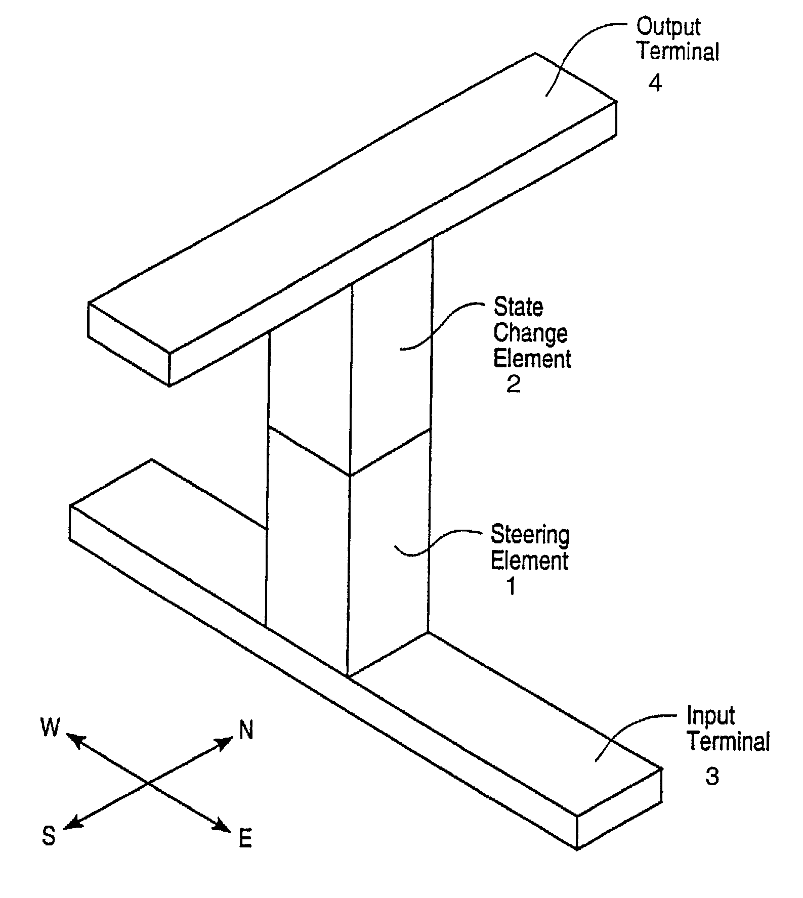
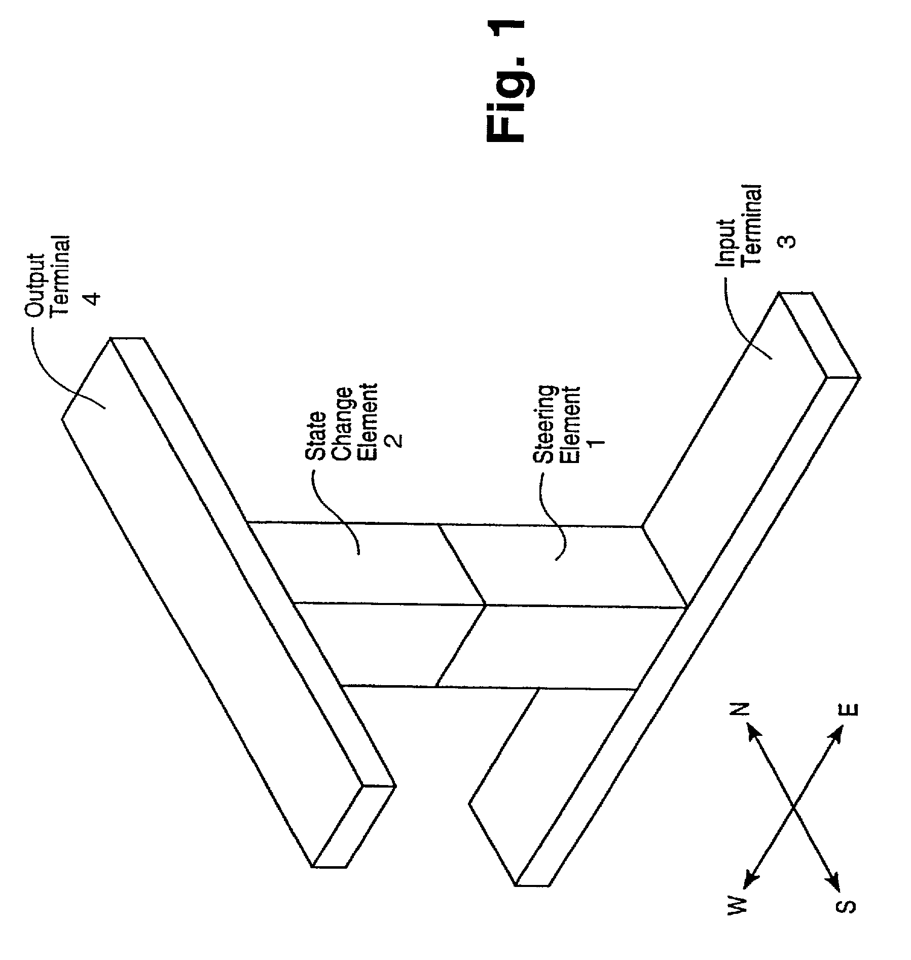
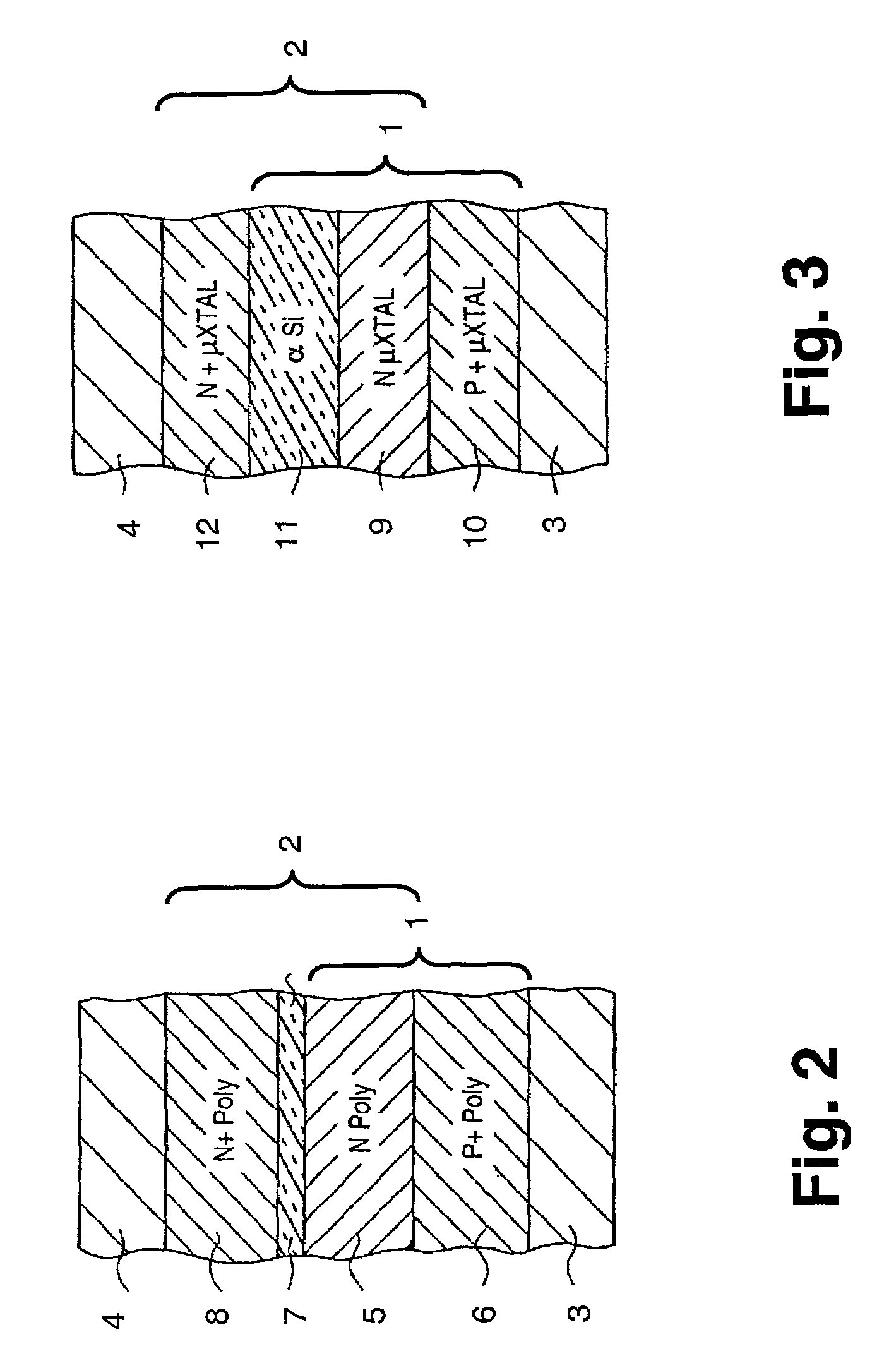
[0018]The present invention provides a hetero-structure, or hetero-junction, suitable for use in diode-based memory circuits. In this regard, the hetero-structures of the present invention provide a higher ratio of forward-to-reverse current compared to homo-structures, or homo-junctions, because a larger energy gap for reverse-flow is achievable between two different semiconductor materials compared to a homo-junction of two layers of a single semiconductor material.

[0019]More generally, each semiconductor material has its own characteristic band gap energy. In a homo-junction structure such as a diode, the asymmetrical conduction characteristics of the diode are entirely a function of doping levels between the junction. In a hetero-structure junction, there is an additional degree of freedom provided by the difference in band gap energies between the different junction materials. Thus, even between two n-doped regions of hetero-junction, there can be asymmetrical conduction if the...


PUM


Abstract

Hetero-structure semiconductor devices having first and second-type semiconductor junctions are disclosed. The hetero-structures are incorporated into pillar and rail-stack memory circuits improving the forward-to-reverse current ratios thereof.

Description

FIELD OF THE INVENTION[0001]The invention relates generally to electronic devices and, more particularly, to memory semiconductor devices having diverse band gap energy levels providing high forward-to-reverse current ratios.BACKGROUND OF THE INVENTION[0002]Memory circuits are at the core of any computer system. In this regard, one of the driving forces in memory circuit design has been to place a maximum number of memory cells in as small a physical space as possible. Initially, memory circuit design was constrained by the planar nature (i.e., two-dimensional) of the physical substrates upon which memory cells were fabricated. This constraint has given way to three-dimensional spaces that include the area provided by the physical substrates and the space above and below such substrates. As such, memory circuit designers introduced vertical memory cells resulting in three-dimensional memory arrays.[0003]Vertical memory cells have themselves evolved into various forms. For example, U...

Claims


Application Information

Patent Timeline
IPC IPC(8): H01L29/861G11C11/36H01L23/525H01L27/10H01L29/165H01L29/205H01L29/267
CPCG11C11/36H01L27/10H01L29/8615H01L29/205H01L29/267H01L29/165H01L23/5252H01L2924/0002H01L2924/00
Inventor LEE, THOMAS H.
Owner SANDISK TECH LLC
Why Eureka
Try Eureka