Method of manufacturing a light emitting device and thin film forming apparatus

a technology of light emitting devices and thin film forming equipment, which is applied in the manufacture of electric discharge tubes/lamps, identification means, instruments, etc., can solve the problems of short circuits between cathodes, leakage current flows in short circuit locations, and the organic compound layer may not be formed on the electrod

Inactive Publication Date: 2002-10-03
SEMICON ENERGY LAB CO LTD
View PDF4 Cites 59 Cited by
  • Summary
  • Abstract
  • Description
  • Claims
  • Application Information

AI Technical Summary

Problems solved by technology

However, if there are defects in a portion of the organic compound layer due to any reason, then short circuits occur between the cathode and the anode, and a leak current flows in the short circuit locations.
In addition, there is a case in which the organic compound layer may not be formed enough on the electrode because there is dust on the electrode.
This causes light emitting elements that have defect portions to emit light at a lowered brightness, or to turn o

Method used


Image

  • Method of manufacturing a light emitting device and thin film forming apparatus
  • Method of manufacturing a light emitting device and thin film forming apparatus
  • Method of manufacturing a light emitting device and thin film forming apparatus

Examples


embodiment 1

[0065] Embodiment 1

[0066] An example of using the present invention in an active matrix light emitting device having two thin film transistors (TFTs) in each pixel will be explained in Embodiment 1.

[0067] FIG. 3 is a circuit diagram of a pixel in a light emitting device in which detection and repair of defect portions of a light emitting element is performed using the present invention. Each pixel has a source signal line Si (where i is any one of 1 to x), an electric current supply line Vi (where i is any one of 1 to x), and a gate signal line Gj (where j is any one of 1 to y).

[0068] Further, each pixel has a switching TFT 301, an electric current control TFT 302, a light emitting element 303, and a capacitor 304.

[0069] A gate electrode of the switching TFT 301 is connected to the gate signal line Gj. Further, one of a source region and a drain region of the switching TFT 301 is connected to the source signal line Si, and the other one is connected to a gate electrode of the electr...

embodiment 2

[0089] Embodiment 2

[0090] A case of performing all processing up through a sealing process within the same apparatus is explained in Embodiment 2. The aforementioned processes include performing the detection and repair processes of the present invention after forming a pixel electrode (anodes) of a light emitting element on a substrate, then forming an organic compound layer and a cathode, and performing repair immediately after forming the cathode (and before performing sealing) in the case where the light emitting element has a defect portion. Note that although the light emitting element having a structure in which a pixel electrode (anode) is formed on a substrate, and a cathode is then formed after forming an organic compound layer on the pixel electrode is explained in Embodiment 2, it is also possible to implement the present invention for the light emitting element having a structure in which a cathode is formed as a pixel electrode, an organic compound layer is formed on t...

embodiment 3

[0130] Embodiment 3

[0131] Property observed by an emission microscope when a reverse bias voltage is practically applied to a light emitting element having a defect portion is explained in Embodiment 3.

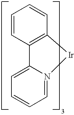
[0132] Light emitting elements used in Embodiment 3 is one in which an anode made from a compound in which indium oxide and tin oxide are combined (ITO) is formed, copper phthalocyanine is formed having a film thickness of 20 nm on the anode by evaporation as a hole injecting layer, and then .alpha.-NPD is formed by evaporation on the hole injecting layer with a thickness of 40 nm as a hole transporting layer. Ir(ppy).sub.3, a triplet compound, is formed on the hole transporting layer as a light emitting material for forming a light emitting layer with a film thickness of 20 nm by common evaporation with CBP. In addition, BCP is formed having a film thickness of 10 nm as an electron injecting layer on the light emitting layer, and a 140 nm thick film of aluminum is formed as a cathode...


PUM


Abstract

A method of manufacturing a light emitting device is provided in which satisfactory image display can be performed by the investigation and repair of short circuits in defect portions of light emitting elements. A backward direction electric current flows in the defect portions if a reverse bias voltage is applied to the light emitting elements having the defect portions. Emission of light which occurred from the backward direction electric current flow is measured by using an emission microscope, specifying the position of the defect portions, and short circuit locations can be repaired by irradiating a laser to the defect portions, turning them into insulators.

Description

[0001] 1. Field of the Invention[0002] The present invention relates to a method of manufacturing a light emitting device containing light emitting elements formed on a substrate, in which locations of short circuits between cathodes and anodes are detected and then repaired. Further, the present invention relates to a method of manufacturing a light emitting device in which locations of short circuits are detected, and then repaired, in a light emitting module wherein an IC is mounted to a light emitting panel manufactured by sealing light emitting elements formed on a substrate, using a sealing substrate. Note that the terms light emitting panel and light emitting module are generic names for light emitting devices throughout this specification. In addition, a thin film formation device capable of manufacturing a light emitting device by detecting the aforementioned short circuit locations and then repairing them is contained within the present invention.[0003] 2. Description of t...

Claims


Application Information

Patent Timeline
IPC IPC(8): G09F9/00H01L51/50H01L51/52H05B33/10H05B33/12
CPCH01L51/52H01L51/0032H01L2251/568Y10T428/31504H10K50/80H10K71/861H10K71/70H10K50/844H10K71/00H10K85/00
Inventor YAMAGATA, HIROKAZUADACHI, YOSHIMISHIBATA, NORIKO
Owner SEMICON ENERGY LAB CO LTD
Why Eureka
Try Eureka