Planar spiral inductor structure with patterned microelectronic structure integral thereto

a microelectronic structure and spiral inductor technology, applied in the direction of semiconductor/solid-state device details, electrical apparatus, semiconductor devices, etc., to achieve the effect of being ready for commercialization

Inactive Publication Date: 2006-05-02
TAIWAN SEMICON MFG CO LTD
View PDF14 Cites 12 Cited by
  • Summary
  • Abstract
  • Description
  • Claims
  • Application Information

AI Technical Summary

Benefits of technology

[0024]A fourth object of the present invention is to provide a method in accord with the first object of the present invention, the s

Problems solved by technology

In that regard, it is typically desirable in the art of microelectronic fabrication, but nonetheless not always readily achievable in the art of microelectronic fabrication, to fabricate microelectronic fabrications having formed therein microelectroni

Method used


Image

  • Planar spiral inductor structure with patterned microelectronic structure integral thereto
  • Planar spiral inductor structure with patterned microelectronic structure integral thereto
  • Planar spiral inductor structure with patterned microelectronic structure integral thereto

Examples


Embodiment Construction

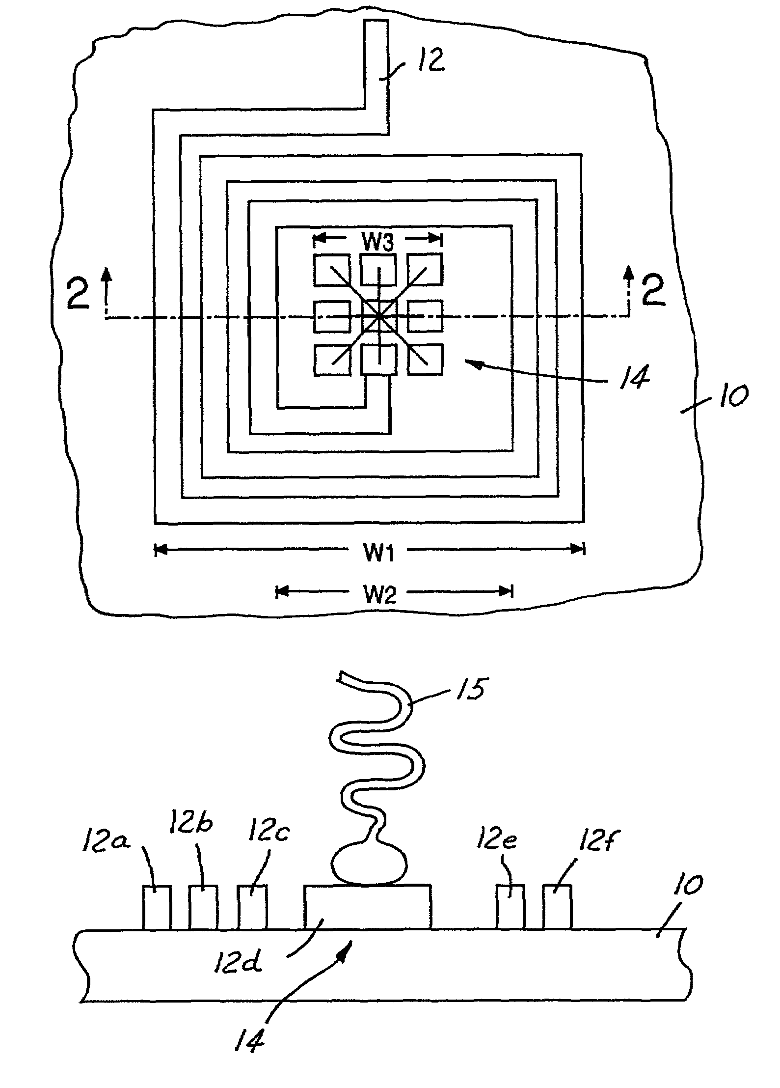
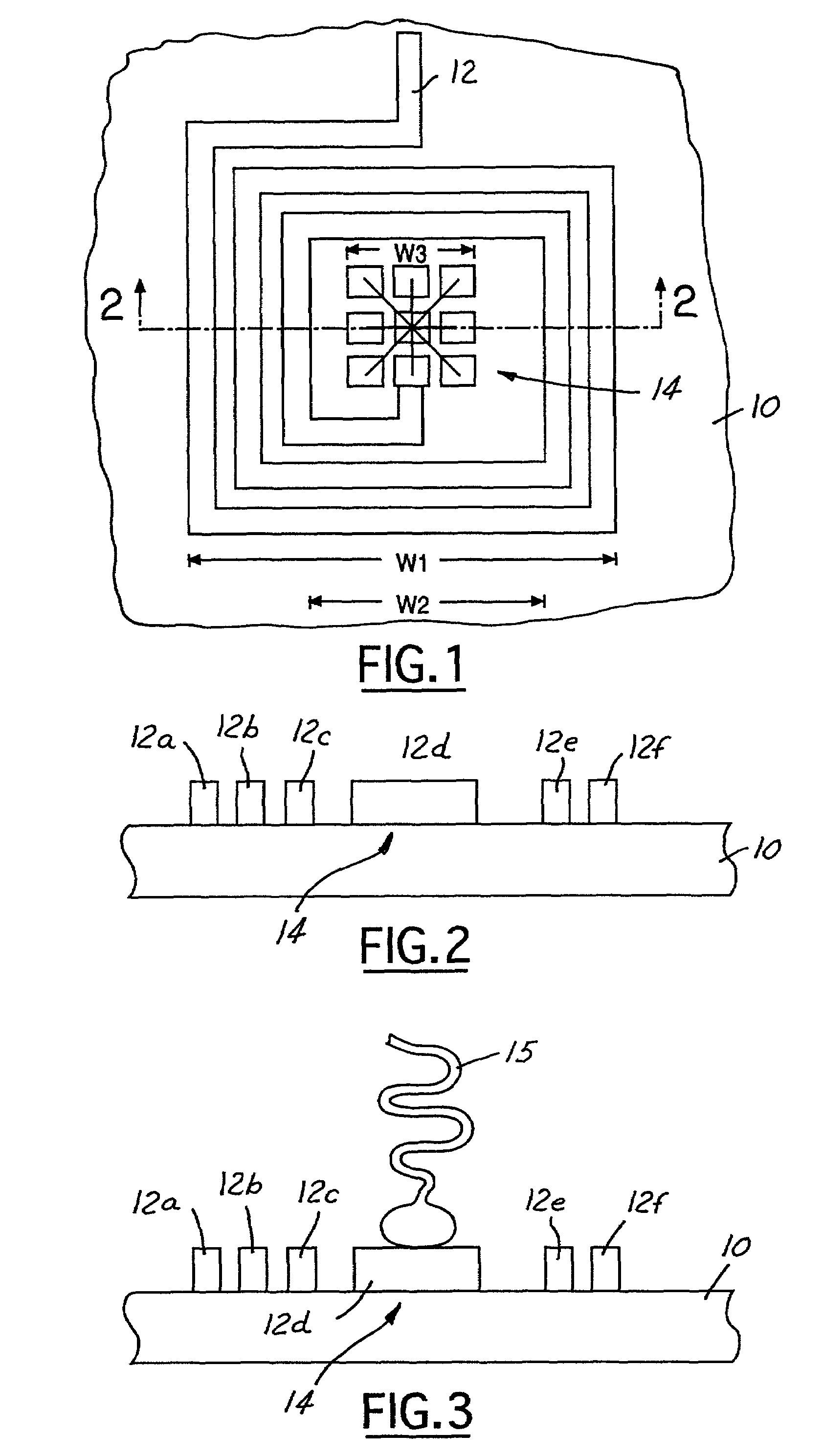
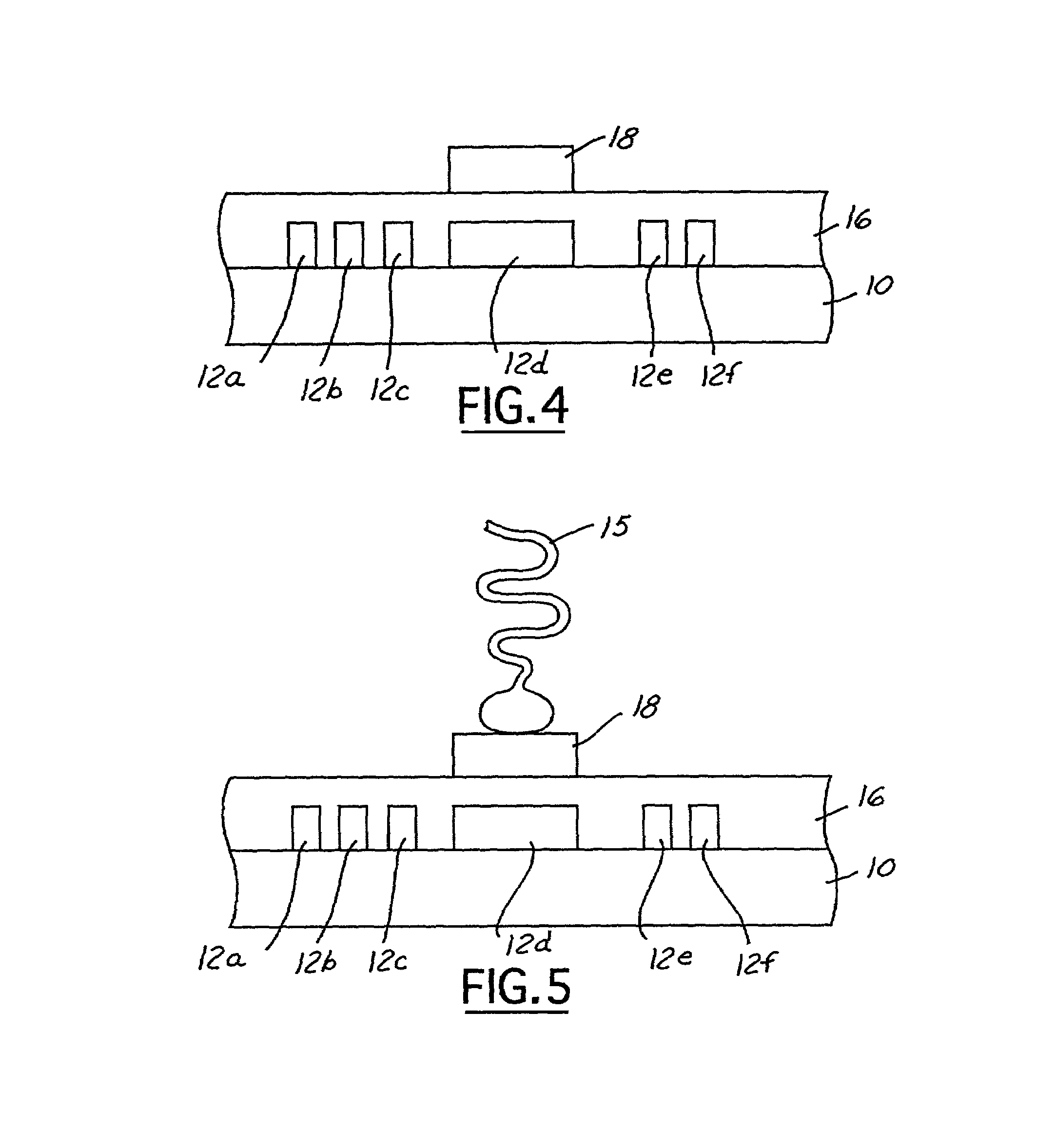
[0035]There is provided by the present invention: (1) a method for fabricating a microelectronic inductor structure within a microelectronic fabrication, as well as the microelectronic inductor structure fabricated within the microelectronic fabrication while employing the method; and (2) a method for fabricating a microelectronic inductor structure in conjunction with a microelectronic capacitor structure within a microelectronic fabrication, as well as the microelectronic inductor structure in conjunction with the microelectronic capacitor structure fabricated within the microelectronic fabrication while employing the method, wherein the microelectronic inductor structure and / or the microelectronic inductor structure in conjunction with the microelectronic capacitor structure are / is fabricated with optimal performance while occupying minimal microelectronic substrate area. A microelectronic inductor structure, or a microelectronic inductor structure in conjunction with a microelec...


PUM


Abstract

Within a method for fabricating a microelectronic fabrication there is first provided a substrate. There is then formed over the substrate a spirally patterned conductor layer which terminates in a microelectronic structure within the center of the spirally patterned conductor layer. The spirally patterned conductor layer forms a planar spiral inductor, and the microelectronic structure formed within the center of the spirally patterned conductor layer further comprises a series of electrically interconnected sub-patterns. The method contemplates a microelectronic fabrication fabricated in accord with the method. The microelectronic fabrication is fabricated with optimal performance while occupying minimal microelectronic substrate area.

Description

CROSS-REFERENCE TO RELATED APPLICATION[0001]This application is related to co-assigned application Ser. No. 09 / 588,788, filed Jun. 6, 2000, titled “Planar Spiral Inductor Structure Having Enhanced Q Value,” the disclosure and references from which related co-assigned application are incorporated herein fully by reference.BACKGROUND OF THE INVENTION[0002]1. Field of the Invention[0003]The present invention relates generally to inductor structures employed within microelectronic fabrications. More particularly, the present invention relates to planar spiral inductor structures employed within microelectronic fabrications.[0004]2. Description of the Related Art[0005]Microelectronic fabrications are fabricated from microelectronic substrates over which are formed patterned microelectronic conductor layers which are separated by microelectronic dielectric layers.[0006]As microelectronic fabrication integration levels and functionality levels have increased, it has become common in the ar...

Claims


Application Information

Patent Timeline
IPC IPC(8): H01L29/00H01L23/485H01L23/522H01L23/64
CPCH01L23/5227H01L24/05H01L24/48Y10S257/909H01L24/45H01L2224/04042H01L2224/05556H01L2224/05624H01L2224/05644H01L2224/05647H01L2224/45015H01L2224/45124H01L2224/45144H01L2224/45147H01L2224/48463H01L2224/49171H01L2924/01013H01L2924/01014H01L2924/01027H01L2924/01029H01L2924/01079H01L2924/01082H01L2924/01083H01L2924/05042H01L2924/14H01L2924/19041H01L2924/19042H01L2924/19043H01L2924/20751H01L2924/20752H01L2924/20753H01L2924/20754H01L2924/30105H01L2924/30107H01L23/645H01L24/49H01L2224/48747H01L2224/48724H01L2224/48847H01L2224/48844H01L2224/48647H01L2224/48644H01L2924/01033H01L2924/01067H01L2224/48624H01L2924/00014H01L2224/48824H01L2924/00H01L2224/48744H01L2924/15787
Inventor MA, SSU-PINHO, YEN-SHIH
Owner TAIWAN SEMICON MFG CO LTD
Why Eureka
Try Eureka