Photoexposure method for facilitating photoresist stripping

Inactive Publication Date: 2003-12-16
TAIWAN SEMICON MFG CO LTD
View PDF11 Cites 0 Cited by
  • Summary
  • Abstract
  • Description
  • Claims
  • Application Information

AI Technical Summary

Benefits of technology

A fourth object of the present invention is to provide a method in accord with the first object of the present invention, the second object of the present invention or the third object of the present invention, which method is readily commercially implemented.
There is provided by the present invention a method for stripping from a microelectronics fabrication a patterned photoresist layer. The method of the present invention realizes the forgoing object by employing when stripping the patterned photoresist layer in accord with the present invention a patterned positive photoresist layer which is employed as a mask layer when processing a target layer formed beneath the patterned positive photoresist layer. A processed patterned positive photoresist layer formed from the patterned positive photoresist layer incident to processing the target layer is then photoexposed to form a photoexposed processed patterned positive photoresist layer which exhibits an enhanced solubility within a solvent which is then employed to strip the photoexposed processed patterned positive photoresist layer from the processed target layer.
The method of the present invention is readily commercially implemented. The present invention employs methods and materials as are otherwise generally known in the art of microelectronics fabrication. Since it is a process ordering and process control within the present invention which provides at least in part the present invention, rather than the existence of methods and materials which provides the present invention, the method of the present invention is readily commercially implemented.

Problems solved by technology

While the use of patterned photoresist layers as mask layers when forming microelectronics devices and patterned microelectronics layers from corresponding blanket microelectronics layers within microelectronics fabrications is thus quite common in the art of microelectronics fabrication, the use of patterned photoresist layers as mask layers when forming microelectronics devices and patterned microelectronics layers from corresponding blanket microelectronics layers within microelectronics fabrications is not without problems within the art of microelectronics fabrication.
Specifically, it is common in the art of microelectronics fabrication for patterned photoresist layers which have been employed as mask layers for forming microelectronics devices and patterned microelectronics layers from corresponding blanket microelectronics layers often to be particularly difficult to strip from a microelectronics device or patterned microelectronics layer whose fabrication is facilitated employing the patterned photoresist layer.

Method used


Image

  • Photoexposure method for facilitating photoresist stripping
  • Photoexposure method for facilitating photoresist stripping
  • Photoexposure method for facilitating photoresist stripping

Examples


second embodiment

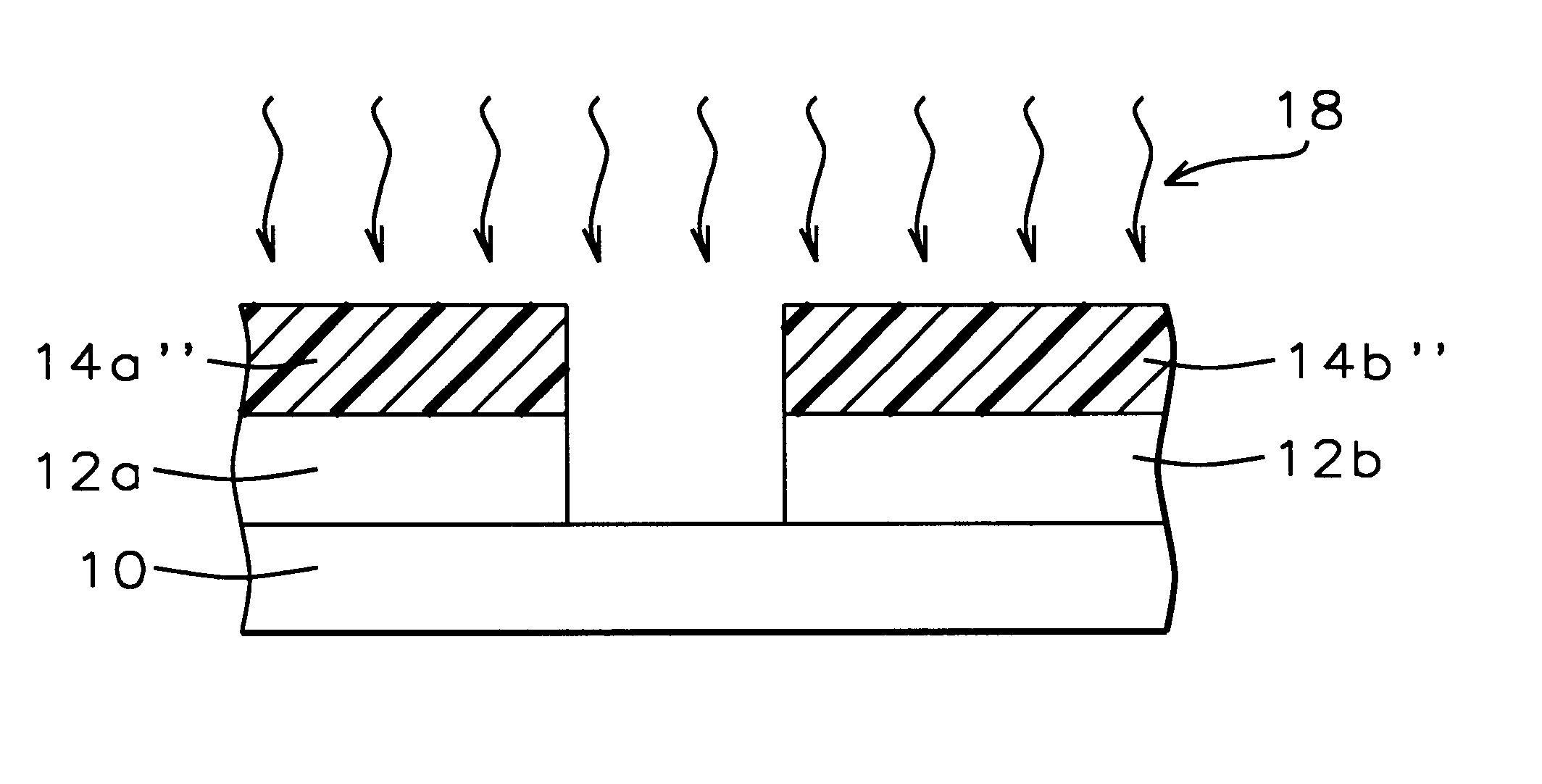
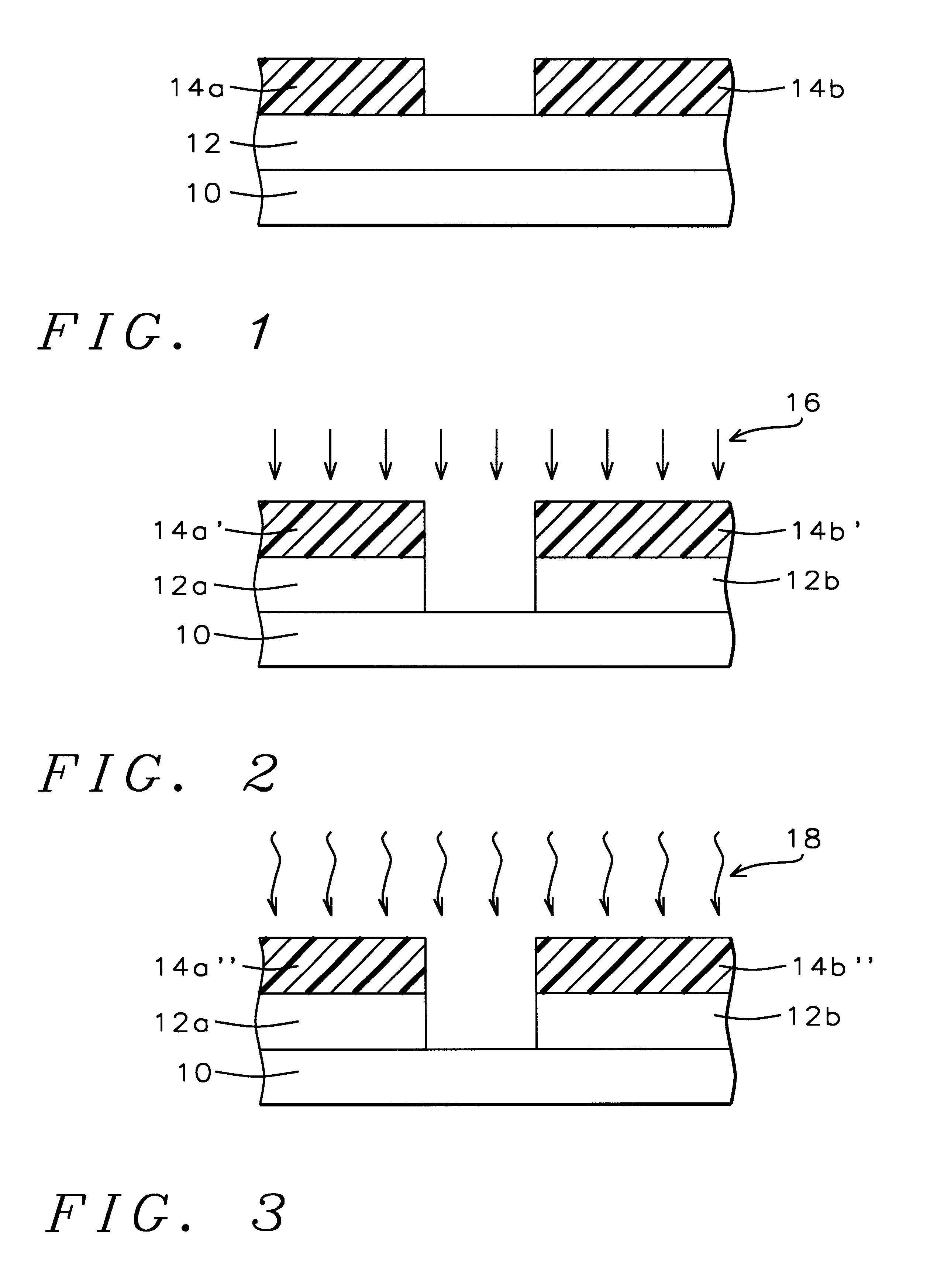
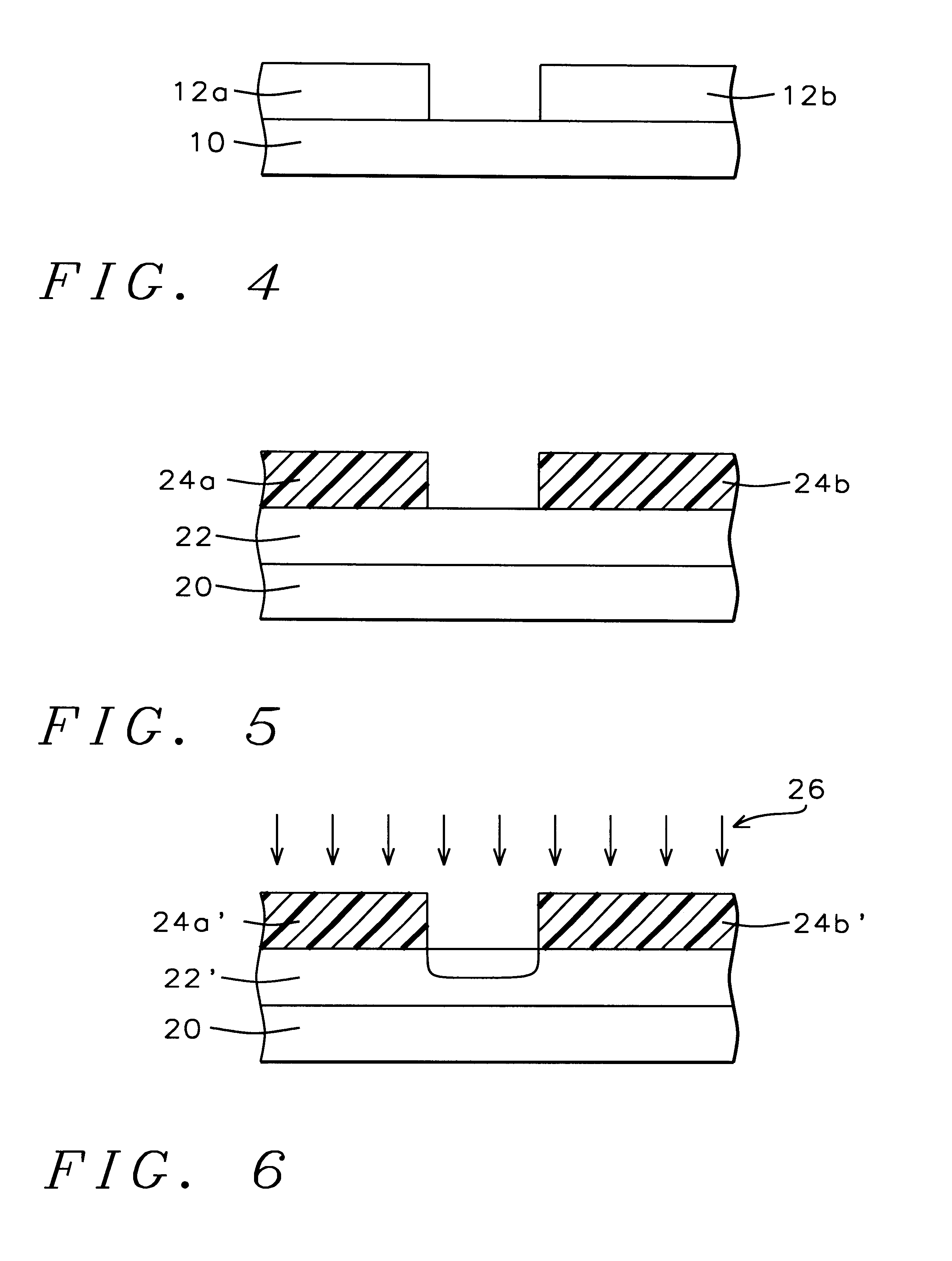
Referring now to FIG. 5 to FIG. 8, there is shown a series of schematic cross-sectional diagrams illustrating the results of progressive stages in forming in accord with a second preferred embodiment of the present invention an ion implanted target layer within a microelectronics fabrication. Shown in FIG. 5 is a schematic cross-sectional diagram of the microelectronics fabrication at an early stage in its fabrication in accord with the second preferred embodiment of the present invention.

Shown in FIG. 5 is a substrate 20 having formed thereupon a blanket ion implantable layer 22 in turn having formed thereupon a pair of patterned photoresist layers 24a and 24b.

Within the second preferred embodiment of the present invention, the substrate 20 is analogous or equivalent to the substrate 10 employed within the first preferred embodiment of the present invention as illustrated in FIG. 1. Similarly, although the ion implantable layer 22 as illustrated within the schematic cross-sectional...


PUM

PropertyMeasurementUnit
Pressureaaaaaaaaaa
Angleaaaaaaaaaa
Angleaaaaaaaaaa

Abstract

There is first provided a substrate 10 and a target layer 12. There is then formed upon the target layer a patterned positive photoresist layer 14. There is then processed the target layer while employing the patterned positive photoresist layer as a mask layer, to thus form a processed target layer and a processed patterned positive photoresist layer. There is then photoexposed 18 the processed patterned positive photoresist layer to enhance its solubility. Finally, there is then stripped from the processed target layer the photoexposed processed patterned positive photoresist layer while employing a solvent.

Description

1. Field of the InventionThe present invention relates generally to methods for stripping photoresist layers employed within microelectronics fabrications. More particularly, the present invention relates to methods for facilitating stripping of photoresist layers employed within microelectronics fabrications.2. Description of the Related ArtMicroelectronics fabrications are formed from microelectronics substrates over which are formed patterned microelectronics conductor layers which are separated by microelectronics dielectric layers.In the process of forming microelectronics devices and patterned microelectronics layers, such as but not limited to patterned microelectronics conductor layers, within microelectronics fabrications, it is common in the art of microelectronics fabrication to employ patterned photoresist layers as mask layers for forming those microelectronics devices and patterned microelectronics layers from corresponding blanket microelectronics layers.While the use...

Claims


Application Information

Patent Timeline
IPC IPC(8): G03F7/42H01L21/02H01L21/027H01L21/311
CPCG03F7/42H01L21/31138H01L21/0274G03F7/422Y10S438/949
Inventor CHEN, DIAN-HAUPENG, CHIANG-JENCHIU, WEI-KAY
Owner TAIWAN SEMICON MFG CO LTD
Why Eureka
Try Eureka