Lateral etch inhibited multiple etch method for etching material etchable with oxygen containing plasma

a multiple etching and oxygen-containing plasma technology, applied in the field of dielectric layers, can solve problems such as not without problems, and achieve the effects of convenient commercial implementation, enhanced resistance of etched patterns, and convenient commercial implementation

Inactive Publication Date: 2005-07-21
TAIWAN SEMICON MFG CO LTD
View PDF33 Cites 4 Cited by
  • Summary
  • Abstract
  • Description
  • Claims
  • Application Information

AI Technical Summary

Benefits of technology

[0018] A third object of the present invention is to provide a method in accord with the first object of the present and / or the second object of the present invention, where the invention is readily commercially implemented.
[0019] In accord with the objects of the present invention, there is provided a method for etching HSQ dielectric layers employed within a microelectronics fabrication with attenuated degradation after etching from photoresist stripping operations. To practice the method of the present invention, there is first provided a substrate. There is then formed over the substrate a low dielectric constant dielectric layer employing silsesquioxane (HSQ) dielectric spin-on-glass (SOG) material. There is then formed over the HSQ dielectric layer a second dielectric layer to form a dual level dielectric layer stack layer. There is then formed over the dielectric layer stack layer a patterned photoresist etch mask layer. The pattern is transferred into and through the dielectric layer stack layer employing a reactive ion subtractive etching environment to etch the pattern through the patterned photoresist etch mask layer. Near the end of the etching cycle, there is added to the etchant environment additional gases under conditions so as to form a plasma in the gas mixture, which enhances the resistance of the etched pattern of the dielectric layer stack layer and attenuates degradation of the dielectric layer during subsequent stripping of the photoresist etch mask layer employing dry plasma ashing and chemical methods.

Problems solved by technology

While plasma ashing combined with solvent methods are in general satisfactory for removal of photoresist residues, they are not without problems.

Method used


Image

  • Lateral etch inhibited multiple etch method for etching material etchable with oxygen containing plasma
  • Lateral etch inhibited multiple etch method for etching material etchable with oxygen containing plasma
  • Lateral etch inhibited multiple etch method for etching material etchable with oxygen containing plasma

Examples


first preferred embodiment

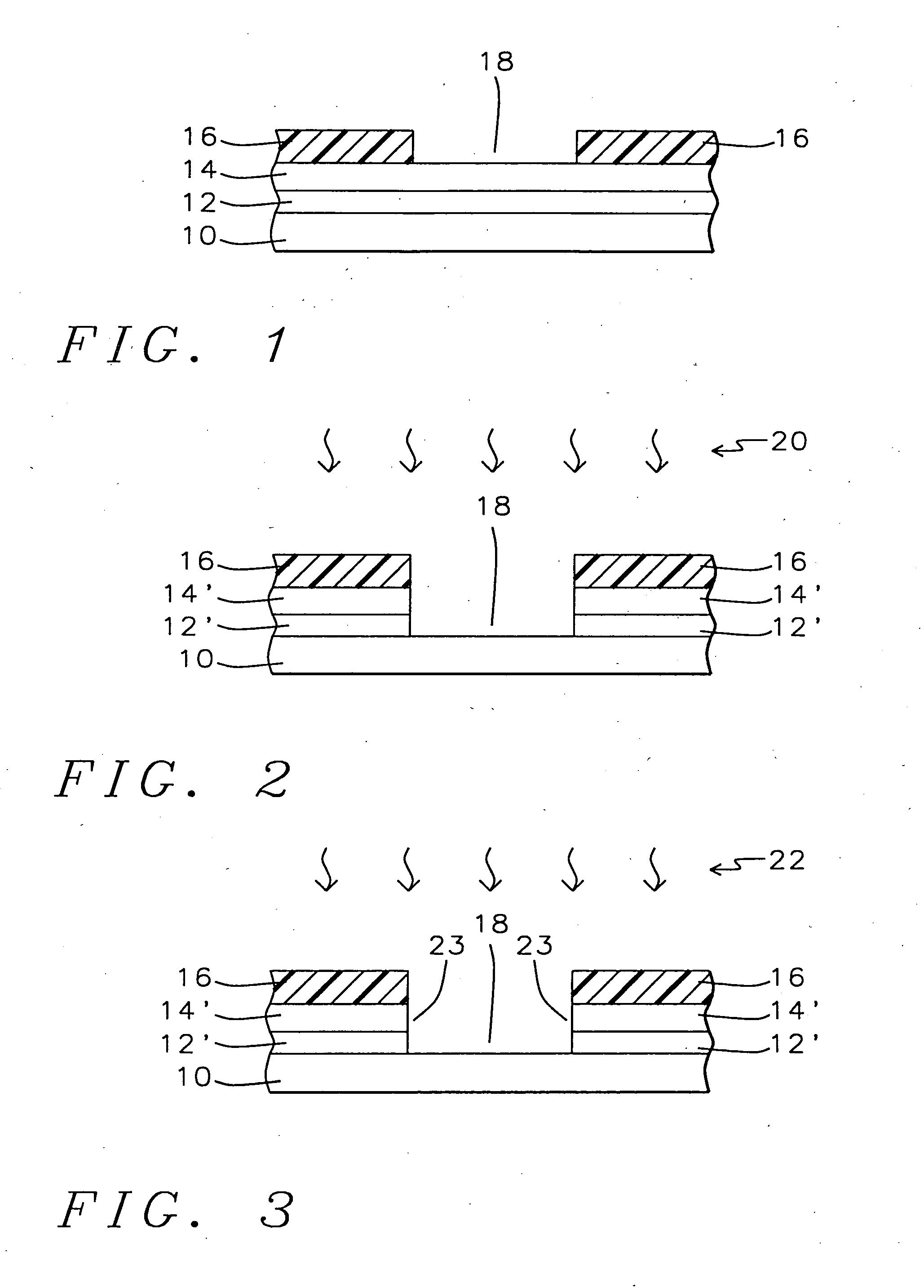
[0025] Referring now more particularly to FIG. 1 to FIG. 4, there is shown the results of etching, within a dual layer stack dielectric layer formed over a substrate employed within a microelectronics fabrication, a pattern employing a patterned photoresist etch mask layer with attenuated degradation due to subsequent stripping of the photoresist mask layer. Shown in FIG. 1 is a schematic cross-sectional diagram of a microelectronics fabrication at an early stage in its fabrication in accord with a first preferred embodiment of the present invention.

[0026] Shown in FIG. 1 is a substrate 10 upon which is formed a first dielectric layer 12 and a second dielectric layer 14 to form a dual layer stack dielectric layer. Formed over the dual layer stack dielectric layer is a photoresist etch mask layer 16 formed into a pattern 18.

[0027] With respect to the substrate 10 shown in FIG. 1, the substrate 10 may be a substrate employed within a microelectronics fabrication selected from the gr...

second preferred embodiment

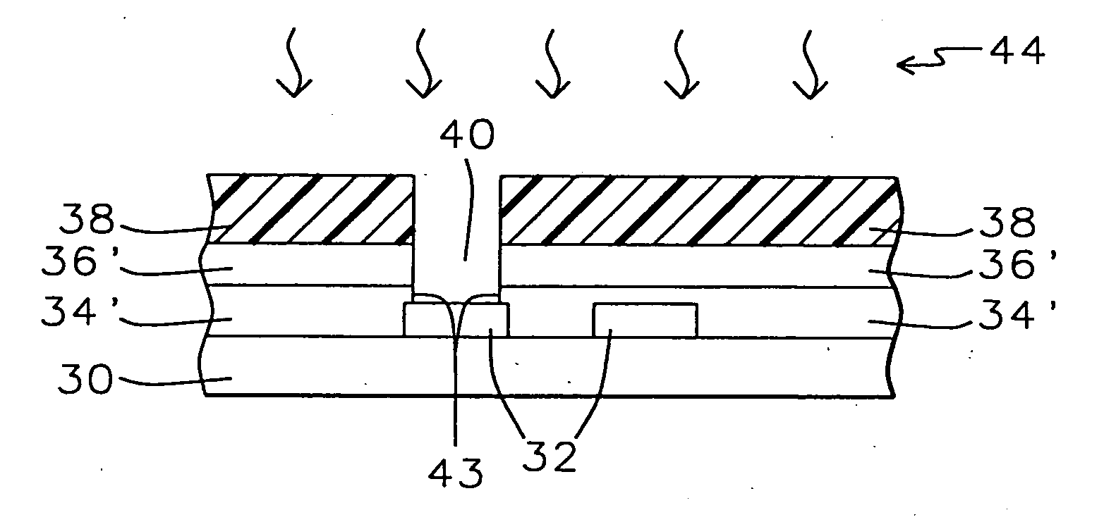
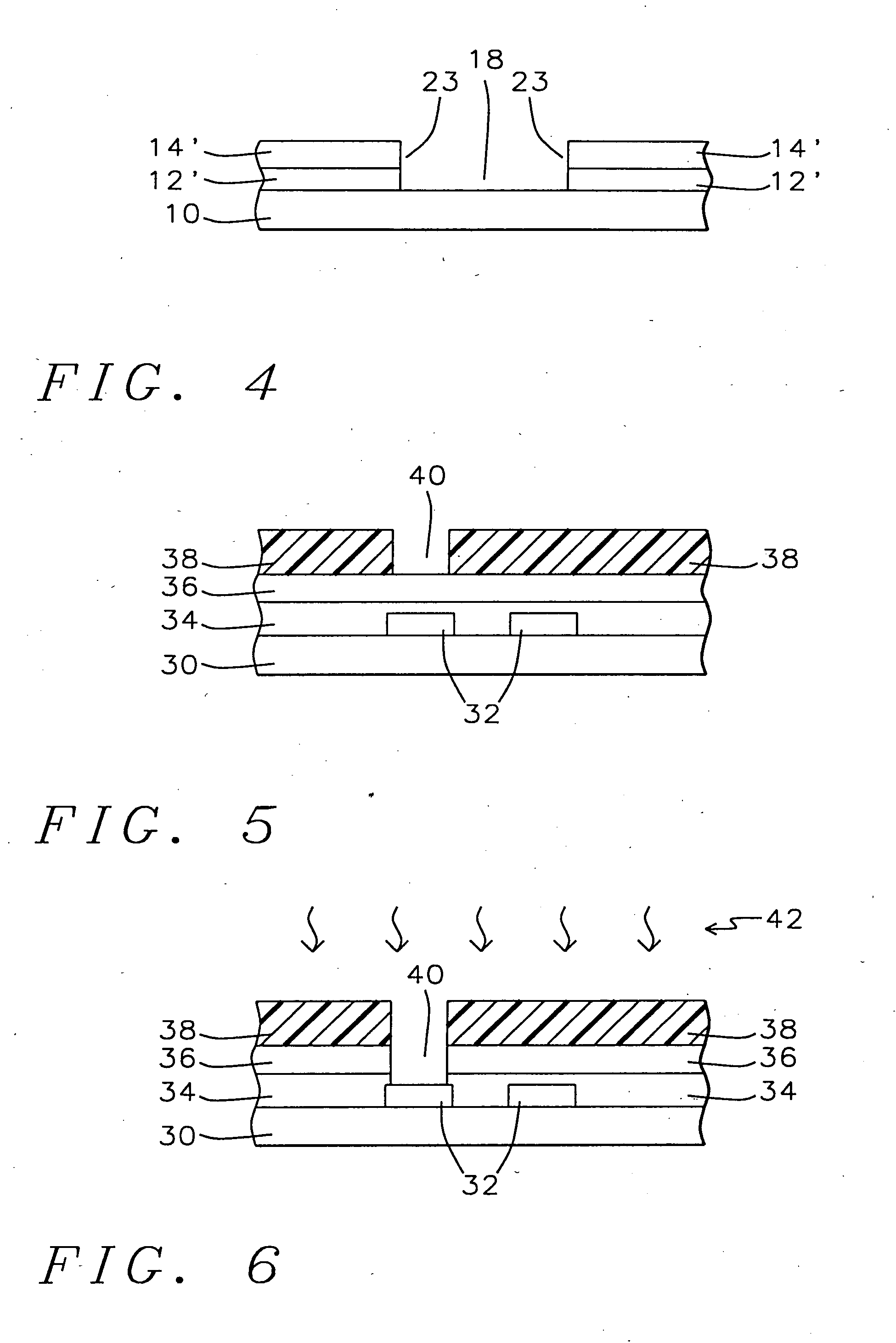
[0038] Referring now more particularly to FIG. 5 to FIG. 9, there is shown a series of schematic cross-sectional diagrams illustrating the results of etching within an inter-level metal dielectric (IMD) layer with reduced inter-level capacitance formed upon a substrate employed within an integrated circuit microelectronics fabrication a pattern employing etching conditions to provide attenuated degradation to the etched pattern by subsequent stripping of the photoresist etch mask layer employing plasma etching and chemical methods. FIG. 5 shows a schematic cross-sectional diagram of an integrated ciruit microeelctronics fabrication at an early stage of its fabrication in accord with a second preferred embodiment of the present invention.

[0039] Shown in FIG. 5 is a semiconductor substrate 30 having formed over it a microelectronics patterned layer 32. Formed over the substrate is a planar blanket first dielectric layer 34. Formed over the first blanket planar dielectric layer is a s...


PUM

PropertyMeasurementUnit
pressureaaaaaaaaaa
thicknessaaaaaaaaaa
thicknessaaaaaaaaaa

Abstract

A method for etching a pattern within a dual-layer stack dielectric layer employed within a microelectronics fabrication. A first low dielectric constant dielectric layer employing HSQ polymer spin-on-glass (SOP) dielectric material is formed over a substrate. A second dielectric layer is then provided to form a dual level dielectric stack layer. There is then formed over the dual dielectric layer a patterned photoresist etch mask layer. The pattern is transferred into and through the dielectric stack layer employing an anisotropic reactive ion etching environment to etch the pattern through the patterned photoresist etch mask layer. There is then added to the etchant environment additional gases under conditions to form a plasma in the final etching environment to stabilize the etched pattern surface and attenuate degradation of the etched pattern during subsequent stripping of the photoresist etch mask pattern.

Description

RELATED APPLICATION [0001] This application is a continuation of U.S. patent application Ser. No. 09 / 419,105 filed Oct. 15, 1999, and entitled, “Lateral Etch Inhibited Multiple Etch Method for Etching Material Etchable,” which is hereby incorporated by reference in its entirety.BACKGROUND OF THE INVENTION [0002] 1. Field of the Invention [0003] The invention relates to the field of dielectric layers employed within microelectronics fabrications. More particularly, the invention relates to the etching of dielectric layers and the removal of photoresist etch mask residues employed therein in microelectronics fabrications. [0004] 2. Description of the Related Art [0005] The fabrication of microelectronics devices employs surface layers of materials deposited upon substrates and fashioned into patterns to form the substructures of the final microelectronics fabrication. An essential part of the fabrication process is that of photolithography, wherein finely-detailed patterns are transfe...

Claims


Application Information

Patent Timeline
Patent Type & Authority Applications(United States)
IPC IPC(8): G03C5/00H01L21/311H01L21/768
CPCH01L21/31116H01L21/76802H01L21/31138
Inventor LIU, JEN-CHENGYANG, SHU-CHIHTAO, HUN-JANTSAI, CHIA-SHIUNG
Owner TAIWAN SEMICON MFG CO LTD
Why Eureka
Try Eureka